Introduction to AI Semiconductors: Mastering Everything with Excel, No EDA Tools Required

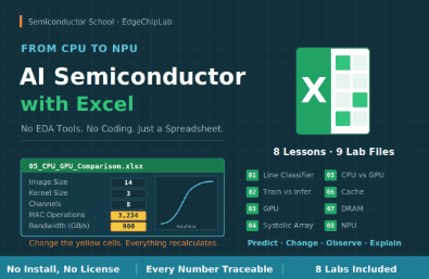
Did you give up while learning Verilog and EDA tools? A semiconductor professor who designs NPUs himself will show you how to understand everything from CPUs to NPUs by calculating with just 9 Excel files.

4 learners are taking this course

Level Beginner

Course period Unlimited

AI
AI
Excel
Excel
Computer Architecture
GPU
GPU
Machine Learning(ML)
AI
AI
Excel
Excel
Computer Architecture
GPU
GPU
Machine Learning(ML)

What you will gain after the course

  • The ability to explain what bottleneck and bandwidth mean in AI semiconductor articles.

  • The ability to explain the differences between CPU, GPU, and NPU based on their structural reasons.

  • Answering ability to not get stuck when asked "Explain the difference between GPU and NPU" in an interview

  • Understanding the differences between DRAM and SRAM through hands-on practice

  • 9 types of AI semiconductor practice Excel files

  • The ability to manually calculate and find the point where performance plateaus even when increasing the number of arithmetic units.

  • The explanatory power of why SRAM is not used as main memory despite being 40 times faster.

■ Without a semiconductor simulator, using only Excel

Attempts to understand AI semiconductors usually stop at a high barrier to entry. You have to learn hardware description languages, install EDA tools, secure licenses, and learn how to interpret waveforms. This process alone takes months, and most of your time is spent learning the tools before you even get a feel for the overall architecture.

This lecture offers a different path. It is designed to implement semiconductor behavior as a calculation model on a spreadsheet, allowing students to directly adjust input values and observe the resulting changes.

Just open the Excel file and change the numbers in the yellow cells.

■ Why Excel can replace EDA tools

The essence of semiconductor simulation is to observe how results change when conditions are altered. The practice files for this lecture perform that function within a spreadsheet.

· No installation required

Excel or a compatible spreadsheet program is sufficient.

There is no need for a separate development environment, license, or setup process.

· The entire calculation process is visible

EDA tools output results as waveforms. The intermediate processes are hidden.

In a spreadsheet, all intermediate values are displayed directly in the cells.

You can directly check which formula was used to produce that value.

· Responds immediately

If you change the value in the input field, the related tables and graphs are updated on the spot.

There is no compiling or waiting for execution.

· Remains even after completing the course

Even after the lecture ends, you can continue to use the files as they are.

You can continue your own experiments by inputting new conditions.

■ These are not static charts

The practice files for this lecture are not tables that merely show pre-calculated results. The execution process of the semiconductor is implemented through formulas, so if the input changes, the entire result is recalculated in a chain reaction.

· By unfolding the process of the CPU executing instructions into 27 steps,

Trace each line to see which values are read and accumulated at each step.

· The point where the GPU's arithmetic unit utilization reaches the bandwidth limit

Calculate it using formulas and verify it through graphs.

· The five stages of charge restoration every time the DRAM reads

Compare it with SRAM by going through it step by step.

· The location where calculations are activated in the systolic array

It tracks the process of moving diagonally over time on a cell-by-cell basis.

· While the NPU's 13×10 arithmetic unit array processes 52 tiles

It calculates the number of memory accesses occurring at each step.

This type of learning material is difficult to find on the market. It was created to fill the gap between introductory books that remain at the level of conceptual diagrams and metaphors, and professional texts that presuppose knowledge of hardware description languages.

■ Eight topics lead to a single problem

This lecture is not a list of independent topics. It is designed with a structure that starts from one question and deepens into the next.

What does artificial intelligence calculate?

What kind of burden arises when performing those calculations with a general-purpose processor?

How does the parallel structure alleviate that burden, and where does it reach its limits?

If memory is the constraint, why not just use faster memory?

What is the reason why high-speed memory cannot be fully adopted?

What changes when data is reused?

What benefits and costs arise when this is implemented as a circuit?

The questions remaining at the end of each session serve as the starting point for the next. Ultimately, you will reach a system design perspective that simultaneously considers performance, power, area, cost, and data movement.

■ Learning Method

Each session includes a process of changing input values. The recommended order is as follows.

First, predict the outcome

After changing the values

observe the actual results,

try to explain the reason why.

Entering values is not the goal itself. The goal is to understand the causal relationship between which inputs affect which results. When expectations and reality do not align, your understanding deepens in the process of finding the reason why.

■ Provided Materials

We provide all 9 types of Excel files used in the lecture.

01_Line_Classifier.xlsx Decision process of a linear classifier

02_MNIST_Learning.xlsx Principles of weight learning

03_Training_and_Inference.xlsx Comparison of computational load between training and inference

04_CPU_Operation.xlsx Instruction Execution and Pipelining

05_CPU_GPU_Comparison.xlsx Parallel Architecture and Memory Bottleneck

06_DRAM_SRAM.xlsx Principles of memory hierarchy formation

07_Systolic_Array.xlsx Data Reuse and Execution Schedule

08_NPU.xlsx Structural Characteristics of Dedicated Accelerators

Each file consists of guidance, main body, conditions, tables, and summary sheets. Input cells are distinguished in yellow, and other areas are protected. You can experiment freely without worrying about damaging the formulas.

■ Target Audience

· Those who come across materials related to AI semiconductors but

Those who wish to systematically organize their technical background

· While preparing for employment in the semiconductor industry

Those who wish to organize their understanding of computer architecture and accelerator concepts

· Those who are non-majors but wish to be able to judge technology trends

Those who wish to acquire foundational knowledge

· Before learning hardware description languages

Those who wish to grasp the overall structure first

· Those who need to explain AI semiconductors in an educational setting

■ Prerequisites

Being able to enter numbers into a spreadsheet is sufficient. No programming experience, semiconductor expertise, or separate development environment is required.

■ Scope of the Lecture Model

The calculation models used in this lecture are simplified for educational purposes and are not intended to predict the performance metrics of actual products.

The conditions assumed for each model are specified on each practice screen, and any differences from actual designs are explained separately during the lecture. The goal is not to memorize the numbers themselves, but to understand the structural reasons why such numbers are derived.

■ Lecture Composition

Total 9 sections · 9 lectures · 3 hours 34 minutes total

Section 1 and Section 2 are available for free.

Recommended for
these people

Who is this course right for?

  • A semiconductor job seeker who wants to grasp the overall structure before learning Verilog and EDA tools.

  • AI developers who want to understand the relationship between model performance and hardware through numerical data

  • An electronics engineering student who wants to verify concepts learned in computer architecture with actual numbers.

  • Educators who need hands-on materials to use when explaining AI semiconductors

  • A semiconductor industry planner who wants to judge technical meetings and documents for themselves.

Need to know before starting?

  • It is enough if you can enter numbers into the spreadsheet.

  • No programming experience or specialized knowledge in semiconductors is required.

  • You will not have to write the formulas yourself. You only need to change the values in the blank cells of the Excel sheet.

Hello
This is EdgeChipLab

Career Verified

Design and implement AI semiconductors directly on FPGAs

As a current university professor, I have incorporated 30 years of experience in the system semiconductor industry, along with expertise in AI semiconductor research and education.

This is a hands-on curriculum designed by a professor who teaches semiconductor engineering, based on direct design and FPGA verification experience—from starting as a systems semiconductor researcher in Samsung Electronics’ DS Division, to serving as a Director at the company’s UK and German subsidiaries, and then leading the System LSI marketing and sales group.

This is not simply a course on how to use FPGAs.
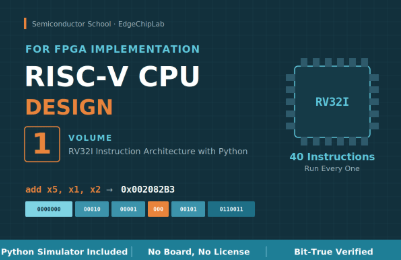
It is designed to help you understand AI algorithms → directly design NPUs and CPUs in RTL → implement them on an FPGA → verify them on actual hardware → and ultimately expand to AI SoCs.

AI Algorithm → RTL Design → FPGA Implementation → Bit-True Verification → AI SoC


Beyond theory to real-world AI hardware implementation

It is difficult to develop system-level AI semiconductor design capabilities with only fragmented, scattered knowledge.

Students do not stop at using finished black-box IP. The goal is to gradually develop the system design skills needed to design an AI NPU and RISC-V CPU themselves, integrate memory and peripherals, and ultimately build their own AI SoC.

Starting with the fundamentals of transistors and digital circuits, you will progress through FPGAs, CPUs, and NPUs to hardware for accelerating Transformers and LLMs.


We validate the research results on actual FPGA hardware.

This is not a lecture you simply watch. Rather than stopping at theory or basic simulations, you will run AI semiconductor circuits you designed yourself on an actual FPGA and perform Bit-True verification to confirm that the Python model and RTL results match down to the last bit.

The instructor’s research findings, including four KCI-listed papers on AI semiconductors, FPGAs, and RISC-V, are also connected to the educational content, enabling technologies validated through research to be applied to actual designs and FPGA implementations.

We make the source code needed for hands-on practice publicly available, including our self-developed RISC-V CPU, Python code for image training, and Verilog RTL.

Centered around the affordable Arty S7-25 FPGA board and the free Vivado design tool, this course is designed to enable learners to reproduce the entire process of designing, implementing, and verifying their own work.

It is also compatible with Digilent FPGA boards, including the Zybo Z7. You can use it by modifying the XDC pin mapping (board) and clock division parameters (RTL) to match the board.

The 'MNIST NPU with FPGA' course only requires modifying the XDC pin mapping, while courses using an OLED and Camera require modifying the clock division parameters (RTL).

→The lecture exercises are configured with clock division parameters based on Arty S7’s 100 MHz input clock. Since other boards have different input clocks (for example, Zybo Z7 has 125 MHz), you will need to recalculate the division values so that the target frequency remains the same. If you miss this part, the screen or video may not display properly, which can easily be mistaken for a code error, so please check it.


A Seamless Full-Stack Roadmap: From the Basics to a mini LLM Accelerator

All the lectures are not independent fragments, but a journey toward completing one vast system.

  • Step 1: AI Theory and Image Processing Fundamentals (including Machine Learning)

  • Step 2: AI Accelerator (NPU) Design and Verification (Including Machine Learning)

  • Step 3: RISC-V CPU Design and System Integration

  • Step 4: Advanced AI SoC Implementation and Expansion into a mini LLM Acceleration Platform (Continuous Content Updates)


Objective verification metrics

All design outcomes from this course have undergone rigorous validation against global standards and by academia.

  • RISC-V Architecture Verification: In-house developed RISC-V CPU, passed the international foundation’s official compliance test (ACT), with source code released publicly (GitHub)

  • Academic Authority: Four sole-authored academic papers (published in the prestigious KCI A-rated journal IJIBC)

  • Global Recognition: Authored and published two global Amazon technology books (reached No. 3 on the bestseller list)

  • Real-world operation verified: Core IPs including the RV32I CPU, NPU, vision system, GPS, Transformer, and AURA-Edge SoC operate flawlessly in the Arty S7 environment.

Take on the challenge. By the time you complete this process of uploading code directly to the board and verifying the results, you will have leveled up into a hardware engineer with a completely different perspective.

More

Curriculum

All

9 lectures ∙ (3hr 33min)

Published: 
Last updated: 

Reviews

Not enough reviews.
Please write a valuable review that helps everyone!

EdgeChipLab's other courses

Check out other courses by the instructor!

Similar courses

Explore other courses in the same field!

Limited time deal

$77,440.00

20%

$74.80