RISC-V CPU Design for FPGA Implementation ③ Building a Full CPU with All 40 RV32I Instructions from Scratch

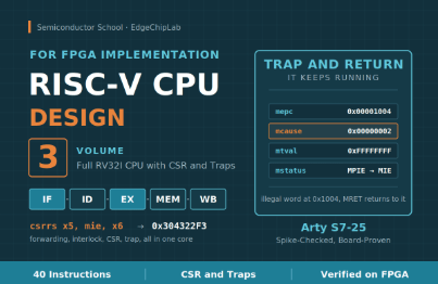
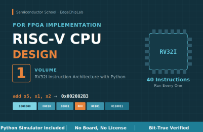
As you study CPUs and RISC-V, you may understand what the instructions do but still find yourself asking, “How are these instructions actually executed in hardware?” and “How can I verify that a CPU I designed myself really works correctly?” Many existing resources stop at ISA explanations or simple CPU examples, and many others rely on completed IP, making it difficult to experience the entire process of designing and verifying a CPU yourself and running programs on an actual FPGA. I have spent many years working in R&D and business in the system semiconductor field, and I have observed this learning gap firsthand while teaching semiconductor design and FPGA at a university. For this reason, rather than providing a completed CPU and simply checking that it operates, this course is structured around designing the CPU directly in a White Box approach, starting with the question, “What hardware is required to execute RV32I instructions?” In Volume 3, we expand Volume 2’s TinyRV32I into a Full-Version 32-bit CPU that uses 40 RV32I instructions. We extend the datapath, Decoder, Branch·Jump, and Byte/Halfword Memory Access, and implement Forwarding and Load-Use Interlock so that the 5-stage Pipeline can handle data dependencies on its own. We then integrate CSR, Exception, Interrupt, Trap, and MRET to complete a CPU capable of handling not only normal program execution but also exceptions and external events. The design does not end with RTL Simulation. You will run actual programs on the CPU, compare the results with the Spike Reference Model, and learn the purpose of the RISC-V Architecture Compatibility Test as well as how to perform and evaluate it through real verification cases. Finally, you will implement the verified CPU on an Arty S7-25 FPGA, receive input from Switches and Buttons, run programs, and confirm the results by displaying them on LEDs. The problem this course aims to solve is not simply learning more RISC-V instructions. Its goal is to connect instructions → CPU architecture → Verilog RTL → Pipeline control → program execution → standards-based verification → actual FPGA operation into a single flow, enabling students to fundamentally understand the internal structure of a CPU and develop the engineering skills to design and verify one themselves.

1 learners are taking this course

Level Intermediate

Course period Unlimited

FPGA
FPGA
verilog
verilog
riscv
riscv
rtl
rtl
cpu-architecture
cpu-architecture
FPGA
FPGA
verilog
verilog
riscv
riscv
rtl
rtl
cpu-architecture
cpu-architecture

What you will gain after the course

  • Ability to design a full-version RISC-V CPU that executes all 40 RV32I instructions

  • Ability to implement a 5-stage pipeline and hazard control

  • Ability to design CPU control structures, including CSR, exceptions, interrupts, and traps

  • Practical skills for systematically verifying CPUs

  • The complete experience of running a self-designed CPU on an FPGA with an actual program

Design your own full-version CPU using the 40 RV32I instructions.

Go beyond a mini-CPU and build a complete 32-bit RISC-V CPU capable of running real programs.

This course covers the process of expanding Volume 2’s TinyRV32I into a Full-Version CPU using the 40 RV32I instructions. Rather than using a completed CPU IP, you will analyze the hardware structures required by the instructions and implement them directly in Verilog RTL.

In addition to arithmetic and logical operations, you will learn how instructions are implemented through the actual datapath and control structure as you expand support to Shift, Compare, Jump, Byte/Halfword Load·Store, CSR, and System instructions.


Expand the 5-stage pipeline into a structure capable of executing actual programs.

As the number of instructions increases, simply expanding the decoder is not enough to complete the CPU.

Expand the ALU, Immediate Generator, Branch/Jump, Load/Store, and Write Back paths, and implement Forwarding and Load-Use Interlock so that the hardware can directly handle data dependencies in programs.

If the required value has already been produced, it is forwarded; if the value is not yet ready, as with a load, the pipeline is temporarily stalled. By implementing PC redirection and flushing for branches and jumps, you will understand how a 5-stage pipeline correctly executes real programs.


Implement Byte/Halfword memory access and MMIO.

Go beyond 32-bit word access by implementing Load and Store operations in Byte and Halfword units.

Handle Sign/Zero Extension, Byte Enable, and Address Alignment, and connect the CPU to the FPGA board’s Switches, Buttons, and LEDs through Memory-Mapped I/O.

Through this, you will understand the entire path of a single Load or Store instruction: address calculation → memory access → data selection → a register or peripheral.


Integrate CSR, Exception, Interrupt, and Trap into the CPU

In addition to normal instruction execution, directly implement exceptions occurring in the CPU and external Interrupts.

Configure Machine-Level CSRs such as mstatus, mtvec, mepc, mcause, mtval, mie, and mip, and handle ECALL, EBREAK, Illegal Instruction, Misaligned Access, External Interrupts, and MRET.

Through this, you will learn at the RTL level how normal program execution → trap occurrence → transfer to the handler → state saving → return to the program takes place within a single CPU.


Verify against standards beyond the in-house Testbench

You cannot conclude that a design is correct simply because the CPU runs a few in-house test programs.

After verifying each function with a Testbench and through Simulation, we compared the execution results with the Spike Reference Model and performed the RISC-V Architecture Compatibility Test and achieved PASS. (See below)
[Compliance Report] EdgeChipLab_CPU_v1 successfully passed RV32I ACT · Issue #1600 · riscv/riscv-arch-test


This section explains an example of verifying this CPU's instruction behavior based on the standard. ACT-related files are not included in the provided materials. Rather than simply checking the PASS result, you will also learn what was executed, what was compared, and the extent to which the results demonstrate the CPU's accuracy.


Run an actual program on the CPU that passed ACT.

This is the biggest distinguishing feature of this course.

A case study in designing a CPU using 40 RV32I instructions, validating it with the Architecture Compatibility Test, and implementing the same CPU on an actual FPGA.

The completed CPU runs an actual program, reads input from the Switches and Buttons, performs computations and branching in the CPU, and then outputs the results to the LEDs.

The entire process is connected as follows.

40-Instruction RV32I → 5-Stage Pipeline → Hazard Control → CSR/Trap → ACT Verification → FPGA → Real Program


We provide hands-on materials needed for CPU design and verification.

The course provides the main design and verification materials used in the lectures, allowing you to run and modify them yourself.

  • Verilog RTL

  • Testbench

  • Assembly Program

  • Memory Image


  • FPGA Top-Level RTL

  • XDC Pin Constraint

  • Vivado Implementation Materials

Rather than simply viewing the completed results, you can reproduce the entire process yourself: design → simulation → standard verification → FPGA implementation.


This is the full-version stage of the RISC-V CPU design series.

This course is the third installment in a step-by-step RISC-V CPU design series.

Volume 1 RV32I Instruction Structure and Execution
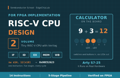
Volume 2 TinyRV32I · 5-Stage Pipeline and FPGA Implementation
Volume 3 40-Instruction Full RV32I · ACT Verification Case Study · FPGA Program Execution ← You Are Here
Volume 4 AI SoC Integrating CPU · NPU · and Peripherals


The goal of this course is not to memorize 40 instructions. It is to share the experience of having a self-designed Full-Version RISC-V CPU pass standards-based verification and to experience the entire process through running programs on an actual FPGA.

Recommended for
these people

Who is this course right for?

  • Hardware engineers who want to learn the fundamentals of RISC-V CPUs and expand into designing a full-version pipelined CPU

  • Developers with RTL design experience who want to practice exception handling and standard verification methods in CPU architecture

  • Those who want to design a more complete CPU themselves, going beyond a simple CPU example

  • Those who want to go beyond simulation and run the CPU they designed on an actual FPGA.

  • Those who want to study the process of integrating multiple RTL blocks into a single system

Need to know before starting?

  • Experience designing and simulating HDL-based RTL using Verilog or VHDL, etc.

  • Basic CPU architecture (Datapath, Control Unit, pipeline) and foundational knowledge of the RISC-V ISA

  • Experience using Vivado or similar FPGA development tools and proficiency in utilizing FPGA boards

Hello
This is EdgeChipLab

Career Verified

Design and implement AI semiconductors directly on FPGAs

As a current university professor, I have incorporated 30 years of experience in the system semiconductor industry, along with expertise in AI semiconductor research and education.

This is a hands-on curriculum designed by a professor who teaches semiconductor engineering, based on direct design and FPGA verification experience—from starting as a systems semiconductor researcher in Samsung Electronics’ DS Division, to serving as a Director at the company’s UK and German subsidiaries, and then leading the System LSI marketing and sales group.

This is not simply a course on how to use FPGAs.
It is designed to help you understand AI algorithms → directly design NPUs and CPUs in RTL → implement them on an FPGA → verify them on actual hardware → and ultimately expand to AI SoCs.

AI Algorithm → RTL Design → FPGA Implementation → Bit-True Verification → AI SoC


Beyond theory to real-world AI hardware implementation

It is difficult to develop system-level AI semiconductor design capabilities with only fragmented, scattered knowledge.

Students do not stop at using finished black-box IP. The goal is to gradually develop the system design skills needed to design an AI NPU and RISC-V CPU themselves, integrate memory and peripherals, and ultimately build their own AI SoC.

Starting with the fundamentals of transistors and digital circuits, you will progress through FPGAs, CPUs, and NPUs to hardware for accelerating Transformers and LLMs.


We validate the research results on actual FPGA hardware.

This is not a lecture you simply watch. Rather than stopping at theory or basic simulations, you will run AI semiconductor circuits you designed yourself on an actual FPGA and perform Bit-True verification to confirm that the Python model and RTL results match down to the last bit.

The instructor’s research findings, including four KCI-listed papers on AI semiconductors, FPGAs, and RISC-V, are also connected to the educational content, enabling technologies validated through research to be applied to actual designs and FPGA implementations.

We make the source code needed for hands-on practice publicly available, including our self-developed RISC-V CPU, Python code for image training, and Verilog RTL.

Centered around the affordable Arty S7-25 FPGA board and the free Vivado design tool, this course is designed to enable learners to reproduce the entire process of designing, implementing, and verifying their own work.

It is also compatible with Digilent FPGA boards, including the Zybo Z7. You can use it by modifying the XDC pin mapping (board) and clock division parameters (RTL) to match the board.

The 'MNIST NPU with FPGA' course only requires modifying the XDC pin mapping, while courses using an OLED and Camera require modifying the clock division parameters (RTL).

→The lecture exercises are configured with clock division parameters based on Arty S7’s 100 MHz input clock. Since other boards have different input clocks (for example, Zybo Z7 has 125 MHz), you will need to recalculate the division values so that the target frequency remains the same. If you miss this part, the screen or video may not display properly, which can easily be mistaken for a code error, so please check it.


A Seamless Full-Stack Roadmap: From the Basics to a mini LLM Accelerator

All the lectures are not independent fragments, but a journey toward completing one vast system.

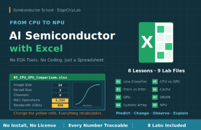
  • Step 1: AI Theory and Image Processing Fundamentals (including Machine Learning)

  • Step 2: AI Accelerator (NPU) Design and Verification (Including Machine Learning)

  • Step 3: RISC-V CPU Design and System Integration

  • Step 4: Advanced AI SoC Implementation and Expansion into a mini LLM Acceleration Platform (Continuous Content Updates)


Objective verification metrics

All design outcomes from this course have undergone rigorous validation against global standards and by academia.

  • RISC-V Architecture Verification: In-house developed RISC-V CPU, passed the international foundation’s official compliance test (ACT), with source code released publicly (GitHub)

  • Academic Authority: Four sole-authored academic papers (published in the prestigious KCI A-rated journal IJIBC)

  • Global Recognition: Authored and published two global Amazon technology books (reached No. 3 on the bestseller list)

  • Real-world operation verified: Core IPs including the RV32I CPU, NPU, vision system, GPS, Transformer, and AURA-Edge SoC operate flawlessly in the Arty S7 environment.

Take on the challenge. By the time you complete this process of uploading code directly to the board and verifying the results, you will have leveled up into a hardware engineer with a completely different perspective.

More

Curriculum

All

11 lectures ∙ (6hr 2min)

Published: 
Last updated: 

Reviews

Not enough reviews.
Please write a valuable review that helps everyone!

EdgeChipLab's other courses

Check out other courses by the instructor!

Similar courses

Explore other courses in the same field!

Limited time deal

$247,500.00

10%

$212.30