inflearn logo

Introduction to Verilog-HDL for Digital Semiconductor Design

You will systematically learn everything from the fundamentals of digital logic circuits to Verilog-HDL syntax, combinational and sequential logic circuit design, and verification through simulation. Drawing on 30 years of experience in Samsung Electronics’ semiconductor division, the instructor will help you clearly understand the relationship between HDL code and actual hardware operation and develop the ability to write synthesizable RTL code.

10 learners are taking this course

Level Beginner

Course period Unlimited

FPGA
FPGA
verilog
verilog
hardware
hardware
circuit
circuit
FPGA
FPGA
verilog
verilog
hardware
hardware
circuit
circuit
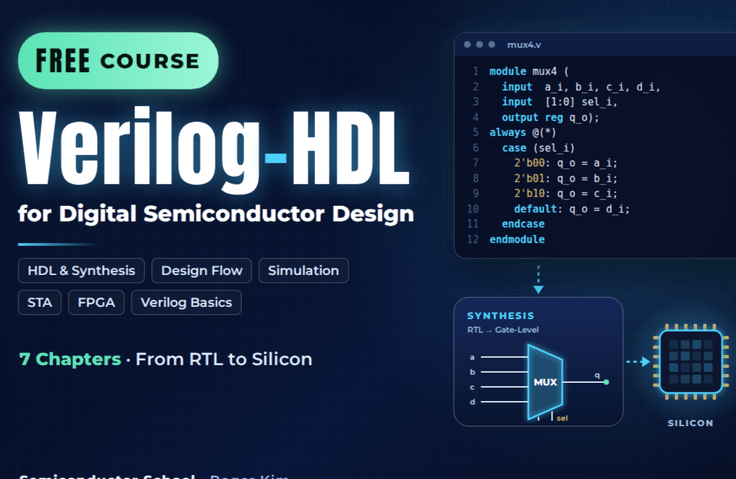
Thumbnail

What you will gain after the course

  • Combinational and Sequential Logic Circuit Design Using Verilog-HDL

  • Testbench development and simulation-based circuit operation verification

  • Writing synthesizable RTL code and understanding the principles of hardware implementation

The first step in digital semiconductor design: Master the fundamentals of Verilog-HDL!

From the semiconductor design flow to Verilog-HDL syntax, testbenches, and RTL design rules!

How are digital semiconductors designed? And how does code written in Verilog-HDL become actual hardware?

To design digital semiconductors such as FPGAs, RISC-V CPUs, and AI NPUs, you must first understand the digital circuit design process and learn Verilog-HDL, a language used to describe hardware.

This course is a free introductory course for systematically learning the overall flow of digital semiconductor design and the core syntax of Verilog-HDL.

It explains everything step by step, from the basic concepts of digital design to RTL coding, behavioral modeling, verification using testbenches, and synthesizable coding practices. It is designed to help learners encountering complex semiconductor design technologies for the first time understand them through concepts and examples.


What You Will Learn in This Course

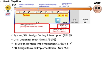
Section 1. Digital Design Flow — Digital Semiconductor Design Flow

Before learning Verilog-HDL, we will examine the process through which digital semiconductors are designed and implemented.

  • Concepts of HDL and RTL (Register Transfer Level)

  • Logic Synthesis and Technology Mapping

  • Behavioral, Structural, and Physical Design Levels

  • The process from RTL design to the gate-level netlist and physical layout

  • Pre-Layout and Post-Layout Verification

  • Basic Concepts of Static Timing Analysis (STA)

  • Understanding the ASIC and FPGA Design Flow

Learning Point: Understand the entire process by which Verilog code is implemented as actual digital hardware.


Section 2. Verilog-HDL Basic Syntax (1) — Basic Syntax for RTL Design

Learn the basic syntax and behavioral modeling methods for expressing digital circuits in Verilog-HDL.

  • Module and Port Declarations and Module Instantiation

  • Structural, Dataflow, Behavioral Modeling

  • Wire, Reg, Bus, and Data Representation

  • Arithmetic, logical, and bitwise operators and number representation

  • Initial and Always Blocks

  • Blocking and Non-Blocking Assignment

  • If/Else, Case, and Loops

  • Design Reuse Using Parameters

  • Register and Memory Array Structures

Learning points: Understand the basic syntax of Verilog-HDL and learn how to express combinational and sequential logic in RTL.


Section 3. Verilog-HDL Basic Syntax (2) — Testbench and RTL Design Rules

Learn how to verify the functionality of the RTL code you write and the basic principles for writing synthesizable Verilog code.

  • The Role and Basic Structure of a Testbench

  • DUT (Device Under Test) and Input Stimulus

  • Clock and Reset Signal Generation

  • Verifying operation through simulation and waveforms

  • Distinguishing synthesizable RTL from simulation-only code

  • Coding Rules for Combinational and Sequential Logic

  • Latch Creation and Race Condition Prevention

  • RTL Coding Style for FPGA Implementation

Learning Points: Understand the basic concepts of testbenches and learn proper RTL coding practices.


Where can it be used?

The Verilog-HDL learned in this course serves as a foundation for various fields of digital semiconductor design.

  • FPGA Design: Digital logic circuit design and hardware implementation using Verilog-HDL

  • ASIC and SoC design: RTL design, logic synthesis, and functional verification

  • RISC-V CPU Design: ALU, Register File, Control Unit, and Processor Design

  • AI NPU Design: MAC unit, datapath, memory, and control circuit design

  • Digital Circuit Verification: Functional verification using Testbench and Simulation


Why did we create this course?

When studying Verilog-HDL to learn FPGA or AI semiconductor design, you may understand the syntax but still find it difficult to determine what hardware the code you write represents. In addition, if you start coding without understanding the actual digital semiconductor design process, it can be difficult to grasp the relationship between RTL design, logic synthesis, simulation, and hardware implementation.

To reduce these learning difficulties, we have organized the entire digital semiconductor design process and the core syntax of Verilog-HDL into a single free course. Drawing on 30 years of practical experience in Samsung Electronics' semiconductor division and experience teaching semiconductor design at the university level, we have focused on the fundamental concepts needed to learn FPGA, CPU, and NPU design.


Recommended for:

  • College students and beginners learning digital semiconductor design for the first time

  • Those who want to systematically learn the basic syntax of Verilog-HDL

  • Learners preparing for FPGA design and implementation practice

  • Those interested in RISC-V CPU and AI NPU/CPU design

  • Aspiring engineers looking to begin learning semiconductor design.

  • Those who wish to take Semiconductor School’s FPGA, NPU, and CPU training courses


After completing the course?

Upon completing this course, you will understand the overall flow of digital semiconductor design and be able to explain the basic syntax of Verilog-HDL and the principles of RTL design. You will also learn the concepts of functional verification using a Testbench and the rules for writing synthesizable RTL code, giving you the foundation needed to proceed to hands-on FPGA design and hardware implementation using Vivado.


Course Information

This course is a free foundational course commonly used across Semiconductor School’s FPGA, RISC-V CPU, and AI NPU design curriculum. It focuses on Verilog-HDL syntax and digital design concepts, while hands-on FPGA board implementation and application projects are covered in separate practical courses.

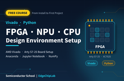
Learners who need to install the Vivado and Python development environments are encouraged to also take the first free course, “FPGA·NPU Hands-on Preparation | Setting Up the Vivado & Python Development Environment”.


From setting up the development environment to learning the basics of Verilog-HDL and designing actual FPGA hardware!

Semiconductor School | EdgeChipLab

Recommended for
these people

Who is this course right for?

  • University students learning semiconductor design for the first time and beginners in electrical engineering

  • Job seeker preparing for positions in RTL design and digital circuit verification

  • For those preparing advanced hardware design projects involving FPGAs, CPUs, NPUs, etc.

Need to know before starting?

  • Basic knowledge of digital circuits and binary numbers (beginner level)

  • Understanding the Basic Concepts of Logic Gates

  • Basic programming experience in C or similar languages (recommended)

Hello
This is EdgeChipLab

Career Verified

Design and implement AI semiconductors directly on FPGAs

As a current university professor, I bring 30 years of experience in the system semiconductor industry, along with expertise in AI semiconductor research and education.

Starting as a system semiconductor researcher in Samsung Electronics’ DS Division, I received the Silver Award (Group Chairman’s Award) in the field of design automation. I later served as Director of Samsung’s UK and German subsidiaries and as Head of the System LSI Marketing and Sales Group, and I currently teach semiconductor engineering. Based on that experience, this curriculum is a hands-on course in which you design systems yourself and verify them on an FPGA.

This is not simply a course on how to use FPGAs.
It is designed to help you understand AI algorithms → directly design NPUs and CPUs in RTL → implement them on an FPGA → verify them on actual hardware → and ultimately extend them to an AI SoC.

AI Algorithm → RTL Design → FPGA Implementation → Bit-True Verification → AI SoC


Beyond theory to real-world AI hardware implementation

With only scattered, fragmented knowledge, it is difficult to develop system-level AI semiconductor design capabilities.

Learners do not stop at using completed black-box IP. They progressively develop the system design skills needed to design an AI NPU and RISC-V CPU themselves, integrate memory and peripherals, port an RTOS on top of them, and ultimately build their own AI SoC.

Starting with the fundamentals of transistors and digital circuits, this course connects FPGA, CPU, and NPU technologies to hardware for accelerating Transformers and LLMs.


We validate the research results on actual FPGA hardware.

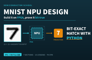
This is not a lecture you only watch. Rather than stopping at theory or simple simulations, you will run AI semiconductor circuits you designed yourself on an actual FPGA and perform Bit-True verification, confirming that the Python model and RTL results match down to the last bit.

We also connect the instructor’s research results, including four KCI-indexed papers on AI semiconductors, FPGAs, and RISC-V, with the educational content, applying technologies validated through research to actual design and FPGA implementation.

We provide source code essential for hands-on practice, including our self-developed RISC-V CPU, Python code for image training, and Verilog RTL.

Centered around the affordable Arty S7-25 FPGA board and the free Vivado design tool, this course is designed to allow learners to reproduce the entire process of designing, implementing, and verifying their own work.

It can also be used with Digilent FPGA boards, including the Zybo Z7. You just need to modify the XDC pin mapping (board) and clock division parameters (RTL) to match the board.

The “MNIST NPU with FPGA” course only requires modifying the XDC pin mapping, while the courses using the OLED and Camera require modifying the clock division parameters (RTL).

→The course exercises are configured with clock division parameters based on Arty S7’s 100 MHz input clock. Since other boards have different input clocks (for example, Zybo Z7 has 125 MHz), you will need to recalculate the division values so that the target frequency remains the same. If you miss this point, the display or video may not output properly, which can easily be mistaken for a code error, so please check this.


A seamless full-stack roadmap: from the basics to a mini LLM accelerator

Every lecture is not an isolated fragment, but part of a journey toward completing one vast system.

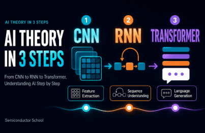
  • Step 1: AI Theory and Image Processing Fundamentals (including Machine Learning)

  • Step 2: AI Accelerator (NPU) Design and Verification (Including Machine Learning)

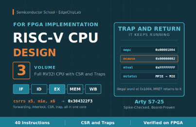
  • Step 3: RISC-V CPU Design and System Integration

  • Step 4: Advanced AI SoC Implementation and Expansion into a mini LLM Acceleration Platform (Continuous Content Updates)


Objective verification metrics

All design deliverables from this course have undergone rigorous validation against global standards and by the academic community.

  • RISC-V Architecture Verification: In-house developed RISC-V CPU, passed the International Foundation’s official compliance test (ACT), and source code released (GitHub)

  • Academic Authority: Four Sole-Author Academic Papers (published in the prestigious KCI A-ranked journal IJIBC)

  • Global Recognition: Published four global Amazon technology books (reached #1 bestseller status)


    Published books: Roger Kim: books, biography, latest update

  • Real-World Operation Verification Complete: Core IPs, including the RV32I CPU, NPU, vision system, GPS, Transformer, and AURA-Edge SoC, operate flawlessly in the Arty S7 environment.


Take on the challenge. By the time you complete this process of uploading code to the board yourself and checking the results, you will have leveled up into a hardware engineer with a completely different perspective than before.

More

Curriculum

All

3 lectures ∙ (1hr 13min)

Published: 
Last updated: 

Reviews

Not enough reviews.
Please write a valuable review that helps everyone!

EdgeChipLab's other courses

Check out other courses by the instructor!

Similar courses

Explore other courses in the same field!

Free