inflearn logo

AI NPU Core Computational Unit Implemented in Verilog | 3×3 Systolic Array Hands-On Practice

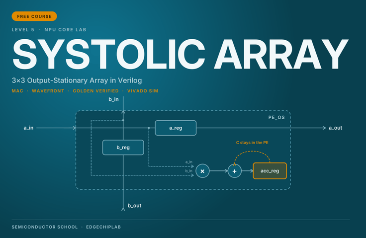
This is a free hands-on course where you implement a Systolic Array—the core parallel computing architecture of AI semiconductors—directly in Verilog and verify it through Vivado simulation. Using a 3×3 Output-Stationary structure as an example, you will learn step by step, from Processing Element design to input skewing, wavefront analysis, and testbench verification, enabling you to fully understand the fundamental computational principles of AI NPUs without an FPGA board.

1 learners are taking this course

Level Basic

Course period Unlimited

FPGA
FPGA
verilog
verilog
cpu-architecture
cpu-architecture
system-verilog
system-verilog
hardware
hardware
FPGA
FPGA
verilog
verilog
cpu-architecture
cpu-architecture
system-verilog
system-verilog
hardware
hardware
Thumbnail

What you will gain after the course

  • Analysis of the Parallel Computation Principles and Data Flow Between PEs in a Systolic Array

  • Design of a 3×3 PE Array and MAC Unit Using Verilog RTL

  • Vivado Simulation and Golden Reference-Based Hardware Verification

Core AI NPU Arithmetic Unit Implemented in Verilog | 3×3 Systolic Array Practice

Implement and verify the parallel computing architecture of AI semiconductors directly in Verilog!

The key to AI semiconductors is processing countless multiplications and additions quickly and efficiently.

Unlike conventional sequential processing, an AI NPU places multiple processing units in parallel to process data simultaneously. A representative hardware architecture for implementing this parallel processing is the Systolic Array (시스톨릭 어레이).

In this course, you will learn how to implement a 3×3 Systolic Array in actual Verilog RTL and verify its operation through Vivado simulation.

Rather than merely explaining the code, we will step by step verify how data moves between the Processing Elements (PEs), which cycle each PE performs its operation, and whether the final result is accurate.

A free hands-on AI NPU design course that you can learn with just Vivado, without an FPGA board.


You will learn the following

Section 1. Systolic Array Architecture and Verilog RTL Design

3×3 Output-Stationary Systolic Array Implementation

Learn the basic structure of a Systolic Array and the principles of parallel matrix multiplication.

In the Output-Stationary structure, input data A and weights B move between PEs, and the multiplication results are stored in the accumulator within each PE.

  • Systolic Array and Output-Stationary Dataflow

  • Processing Element (PE) and MAC Operation Structure

  • Input Data Forwarding and Local Accumulation

  • Signed/Unsigned Data Processing

  • 3×3 PE Array Configuration Using the Generate Construct

Section 2. Systolic Dataflow and Testbench Design

Input Skewing, Wavefront, and Testbench Implementation

In a Systolic Array, data is not simply input simultaneously; instead, the input timing is adjusted so that the data required by each PE arrives at exactly the right moment.

Understand the principles of Input Skewing and the Wavefront, and observe the data flow through the Testbench.

  • Input Skewing and Data Arrival Timing

  • A Wavefront progressing diagonally

  • Computation start times and active periods for each PE

  • Injecting Input Data Using the Testbench

  • Automated Verification Structure Using a Golden Reference

Section 3. Vivado Simulation and NPU Expansion

Golden Data Verification, Performance Analysis, and NPU Expansion

Run the Vivado simulation and verify that the 3×3 matrix multiplication results match the Golden Matrix calculated in Excel.

Analyze the process of 9 PEs performing computations over 7 cycles and understand the characteristics of parallel computation.

  • Vivado Behavioral Simulation

  • Simulation Log and Waveform Analysis

  • PE operation by stage: Fill, Peak, and Drain

  • 7-cycle Wavefront and PE Utilization

  • Compare with the Golden Matrix and verify total_errors = 0

  • Parametric Array Structure and Scalability Concepts

  • Introduction to Quad-Core and CIFAR-10 NPU Application Architectures


What you will gain from this course

1. Understanding the Core Computational Architecture of AI NPUs

You can understand how a Systolic Array uses multiple PEs to process matrix multiplication in parallel.

2. Learn the structure of real-world Verilog RTL designs

Learn how to construct parallel processing hardware using PE, MAC, Forwarding Registers, and Generate statements.

3. Ability to analyze hardware operation cycle by cycle

You can understand Input Skewing and Wavefront, and trace the computation process for each PE through simulation logs and waveforms.

4. Understanding Golden Reference-Based Verification Methods

Learn how to verify the accuracy of hardware operations by comparing RTL simulation results with an Excel Golden Matrix.

5. Foundational Skills for Advanced AI NPU Design

Starting with a 3×3 Systolic Array, you can understand the scaling concepts behind larger PE Arrays and multi-core NPU architectures.


Recommended for these learners

  • Those who want to learn the basics of Verilog-HDL and gain experience with practical hardware design examples

  • University students and beginners who are curious about the internal computational structure of AI semiconductors and NPUs

  • Those interested in parallel computing and digital circuit design using FPGAs

  • Those who want to understand the operating principles of MACs, Processing Elements, and Systolic Arrays

  • Those interested in learning Vivado simulation and testbench-based verification

  • Those who plan to take on the design of AI NPUs, CNN accelerators, and FPGA-based AI systems in the future


Prerequisite Knowledge and Preparation

Recommended Prerequisite Knowledge

  • Basic Concepts of Digital Logic Circuits

  • Verilog-HDL Module, Always, Register, and Generate syntax

  • Operating Principles of Clock-Based Sequential Circuits

  • Basic concepts of matrix multiplication

Practice Environment

  • Xilinx Vivado (Behavioral Simulation)

  • Provided Verilog RTL and Testbench source code

  • No FPGA board required

This course focuses on simulation-based practice and does not include FPGA board implementation or timing closure.


From the basics to real-world AI semiconductor design

This course is a hands-on course covering Systolic Array implementation as part of EdgeChipLab’s step-by-step FPGA and AI semiconductor curriculum.

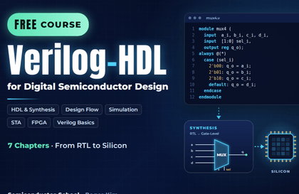
If you are not familiar with Verilog-HDL syntax, we recommend taking the free course “Introduction to Verilog-HDL for Digital Semiconductor Design” first.

Additionally, to fully understand the principles of parallel computation in a Systolic Array, it is recommended to also study the prerequisite theory course, 「Understanding the NPU Systolic PE Architecture」.

Afterward, you can expand your learning through the various FPGA design and AI NPU hands-on courses offered by EdgeChipLab.

See for yourself in this free course how Verilog code becomes actual parallel-computing hardware.

Semiconductor School | EdgeChipLab

Recommended for
these people

Who is this course right for?

  • Hardware beginners who want to learn the basics of Verilog-HDL and gain experience with real-world RTL design examples

  • An electrical and electronic engineering student interested in the internal computational architecture of AI semiconductors and NPUs

  • An engineer focused on FPGA-based parallel computing hardware design and CNN accelerator development

Need to know before starting?

  • Basic Concepts of Digital Logic Circuits and the Operating Principles of Clock-Based Sequential Circuits

  • Basic Verilog-HDL syntax and experience designing modules

  • Basic Concepts of Matrix Multiplication and the Xilinx Vivado Simulator Environment

Hello
This is EdgeChipLab

Career Verified

Design and implement AI semiconductors directly on FPGAs

As a current university professor, I have incorporated 30 years of experience in the system semiconductor industry and expertise in AI semiconductor research and education.

This is a practical curriculum directly designed and verified on an FPGA by a professor who began as a systems semiconductor researcher in Samsung Electronics’ DS Division, went on to serve as a Director at Samsung’s UK and Germany subsidiaries, and later led the System LSI marketing and sales group before becoming a professor teaching semiconductor engineering.

This is not simply a course on how to use FPGAs.
It is designed to help you understand AI algorithms → directly design NPUs and CPUs in RTL → implement them on an FPGA → verify them on actual hardware → and ultimately expand to AI SoCs.

AI Algorithm → RTL Design → FPGA Implementation → Bit-True Verification → AI SoC


Beyond theory to real-world AI hardware implementation

It is difficult to develop system-level AI semiconductor design capabilities with only scattered, fragmented knowledge.

Learners do not stop at using completed black-box IP. The goal is to progressively develop the system design skills to design AI NPUs and RISC-V CPUs themselves, integrate memory and peripherals, and ultimately build their own AI SoC.

Starting with the fundamentals of transistors and digital circuits, you will progress through FPGAs, CPUs, and NPUs to hardware for accelerating Transformers and LLMs.


We validate the research results on actual FPGA hardware.

This is not a lecture you only watch. Rather than stopping at theory or simple simulations, you will run AI semiconductor circuits you designed yourself on an actual FPGA and perform Bit-True verification, confirming that the Python model and RTL results match down to the last bit.

We also connect the instructor’s research results, including four KCI-indexed papers on AI semiconductors, FPGAs, and RISC-V, with the educational content, applying technologies validated through research to actual design and FPGA implementation.

We provide source code essential for hands-on practice, including our self-developed RISC-V CPU, Python code for image training, and Verilog RTL.

Centered around the affordable Arty S7-25 FPGA board and the free Vivado design tool, this course is designed to allow learners to reproduce the entire process of designing, implementing, and verifying their own work.

It can also be used with Digilent FPGA boards, including the Zybo Z7. You just need to modify the XDC pin mapping (board) and clock division parameters (RTL) to match the board.

The “MNIST NPU with FPGA” course only requires modifying the XDC pin mapping, while the courses using the OLED and Camera require modifying the clock division parameters (RTL).

→The course exercises are configured with clock division parameters based on Arty S7’s 100 MHz input clock. Since other boards have different input clocks (for example, Zybo Z7 has 125 MHz), you will need to recalculate the division values so that the target frequency remains the same. If you miss this point, the display or video may not output properly, which can easily be mistaken for a code error, so please check this.


A seamless full-stack roadmap: from the basics to a mini LLM accelerator

Every lecture is not an isolated fragment, but part of a journey toward completing one vast system.

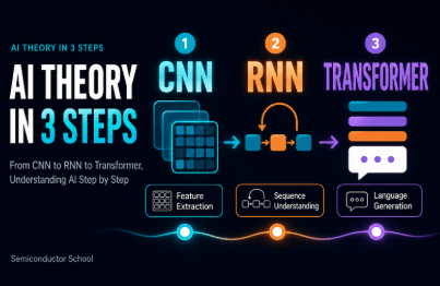
  • Step 1: AI Theory and Image Processing Fundamentals (including Machine Learning)

  • Step 2: AI Accelerator (NPU) Design and Verification (Including Machine Learning)

  • Step 3: RISC-V CPU Design and System Integration

  • Step 4: Advanced AI SoC Implementation and Expansion into a mini LLM Acceleration Platform (Continuous Content Updates)


Objective verification metrics

All design deliverables from this course have undergone rigorous validation against global standards and by the academic community.

  • RISC-V Architecture Verification: In-house developed RISC-V CPU, passed the International Foundation’s official compliance test (ACT), and source code released (GitHub)

  • Academic Authority: Four Sole-Author Academic Papers (published in the prestigious KCI A-ranked journal IJIBC)

  • Global Recognition: Published four global Amazon technology books (reached #1 bestseller status)


    Published books: Roger Kim: books, biography, latest update

  • Real-World Operation Verification Complete: Core IPs, including the RV32I CPU, NPU, vision system, GPS, Transformer, and AURA-Edge SoC, operate flawlessly in the Arty S7 environment.


Take on the challenge. By the time you complete this process of uploading code to the board yourself and checking the results, you will have leveled up into a hardware engineer with a completely different perspective than before.

More

Curriculum

All

3 lectures ∙ (15min)

Published: 
Last updated: 

Reviews

Not enough reviews.
Please write a valuable review that helps everyone!

EdgeChipLab's other courses

Check out other courses by the instructor!

Similar courses

Explore other courses in the same field!

Free