inflearn logo

Everything About Semiconductor Engineering Careers: Finding My Career Path Through an Analysis of Global Company Recruiting

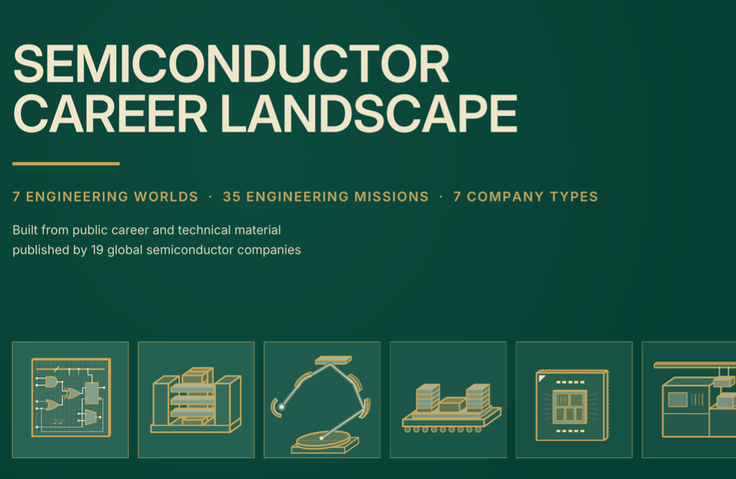
Learn a system of 7 technical fields and 35 engineering roles developed by a semiconductor industry expert with 30 years of experience in Samsung Electronics’ Device Solutions (DS) Division, based on an analysis of recruitment materials from 19 global semiconductor companies. Understand the actual responsibilities and required competencies for each role—from design, processes, devices, and packaging to data analysis—explore career paths available for each major, and develop a job-preparation strategy. ※Lecture language: The lecture slides are provided in English, while the explanations are delivered in Korean. This format is designed to accurately convey the technical terms and job descriptions used in the JDs of global semiconductor companies.

1 learners are taking this course

Level Beginner

Course period Unlimited

Portfolio
Portfolio
asic
asic
leader
leader
career
career
job-analysis
job-analysis
Portfolio
Portfolio
asic
asic
leader
leader
career
career
job-analysis
job-analysis

What you will gain after the course

  • Identify the key responsibilities and required competencies for 35 engineering roles across seven technology areas in the semiconductor industry.

  • Understanding differences in roles and collaboration structures according to business models, such as fabless, memory, foundry, and equipment companies.

  • Explore career paths available based on your major and develop a portfolio-focused job preparation strategy

If you get a job at a semiconductor company, what kind of work will you actually do?

The semiconductor industry encompasses a wide range of companies and numerous engineering roles. Let’s take HBM, which has recently been attracting attention, as an example.

Even if you want to work for a company involved in HBM, it is not easy to know specifically what work you would actually do or how your major connects to particular roles. A single product like HBM involves a wide range of engineering functions, including memory circuit design, device and process development, manufacturing equipment, packaging, testing, yield, and reliability. This structure can be found not only in HBM but also in other semiconductor products.

To understand the semiconductor industry, it is important to go beyond knowing the names of companies and understand what technical problems engineers actually solve.

This course is designed to systematically examine roles across the semiconductor industry and help you connect your major and areas of interest to real-world engineering work.


We analyzed publicly available job information from 19 global semiconductor companies.

The instructor worked in Samsung Electronics’ semiconductor division for approximately 30 years and currently teaches students at a university. Drawing on experience in both industry and university education, the instructor researched and compared public recruitment materials, job descriptions (Job Description, JD), and technical documents from 19 major companies that make up the global semiconductor supply chain.

The analysis includes semiconductor design companies, memory and system semiconductor manufacturers, foundries, semiconductor manufacturing equipment companies, electronic design automation and semiconductor IP companies, and companies specializing in packaging and testing. The 19 companies analyzed and their main business areas are as follows.
The course materials are in English. This is intended to convey, as closely as possible to the originals, the technical terms and job-related expressions used in the Job Descriptions (JDs) of global semiconductor companies. Since the lectures are delivered in Korean, they are structured so that learners who are not familiar with English can also understand the content.


1. Memory Companies (3)

Samsung Electronics, SK hynix, Micron Technology

Key businesses: Design and manufacturing of memory semiconductors such as DRAM, NAND Flash, and HBM, as well as related product technologies

2. System Semiconductor (IDM) and Foundry Companies (2 companies)

Intel, TSMC

Main business: Design and manufacturing of processors and system semiconductors, and contract semiconductor manufacturing (Foundry)

3. Fabless Companies (4 companies)

NVIDIA, Qualcomm, MediaTek, Broadcom

Key Businesses: Design of GPUs, AI accelerators, mobile processors, communications and networking semiconductors, and system semiconductors

4. Semiconductor Manufacturing Equipment and Process Control Companies (5 companies)

ASML, Applied Materials, Lam Research, KLA, Tokyo Electron

Core businesses: lithography, deposition, etching, metrology, inspection, and semiconductor manufacturing equipment and process control technologies

5. Semiconductor Design Automation and IP Companies (3 companies)

Synopsys, Cadence, Siemens EDA

Core businesses: Electronic design automation (EDA), semiconductor design and verification software, and related IP technologies

6. Semiconductor Packaging and Testing Companies (2 companies)

ASE Technology, Amkor Technology

Main business: Semiconductor packaging, assembly, product testing, and advanced packaging technologies


These companies play different roles in the semiconductor supply chain. Some focus on semiconductor design, while others specialize in manufacturing processes, equipment, design software, packaging, and testing. In this way, the semiconductor industry is a global industrial ecosystem that connects various technological fields and specialized companies. Although each company’s business areas and organizational structures differ, the technical problems engineers solve and the specialized capabilities required share common characteristics.

The instructor analyzed these commonalities and differences and systematically organized semiconductor engineering work into 7 Worlds and 35 Missions. This classification is not a direct reproduction of the industry’s official job categories or any individual company’s organizational structure, but rather an educational framework developed by the instructor based on publicly available materials from 19 companies.

Through this, learners can go beyond simply knowing company names or job titles and systematically understand what technical problems engineers actually solve and how their majors and skills can be applied to specific tasks.


The 7 technical fields covered in this course

First, semiconductor chip design

We examine system architecture, digital circuit design, analog and mixed-signal design, physical design, design verification, and design-for-testability.

Second, semiconductor devices and processes

It covers device engineering, process integration, unit process development, and materials engineering.

Third, semiconductor manufacturing technology

We explain computational lithography, metrology, defect inspection, process control, semiconductor equipment, and systems engineering.

Fourth, system integration and packaging

We explore package architecture, assembly processes, and multiphysics co-design that considers electrical, thermal, and mechanical properties together.

Fifth, semiconductor product engineering

It covers silicon validation, testing, product engineering, yield, reliability, failure analysis, and quality engineering.

Sixth, semiconductor manufacturing operations

It covers production operations and factory equipment and infrastructure technology.

Seventh, software, data, and customer engineering

We cover system software, firmware, equipment control software, manufacturing software, semiconductor data and artificial intelligence, EDA, design support, and customer application engineering.

Understand how different roles are connected through an actual semiconductor product

Rather than merely explaining individual roles, we use HBM, or high-bandwidth memory, as a real-world case study to explore how various engineering fields are connected throughout the development of a single product. Achieving HBM performance requires technical decisions across a range of areas, including not only memory design but also devices and processes, packaging, electrical connections, thermal management, testing, and reliability.

Through this example, you can understand the diversity of work performed at companies related to HBM and explore which technical fields your major may be connected to. Furthermore, it provides a perspective that can be applied to other semiconductor products using the same analysis method.

Which semiconductor roles might be connected to my major?

The semiconductor industry involves engineers from a wide range of majors, not just electrical engineering.

Electrical engineering can be connected to circuit and system design; computer engineering to software and design automation; mechanical engineering to equipment and thermal and structural analysis; materials engineering to devices and packaging materials; chemical engineering to manufacturing processes and surface reactions; physics to devices, optics, and measurement; and industrial engineering and data-related fields to manufacturing optimization and data analysis.

The course explains these connections between academic disciplines and introduces the foundational knowledge required for each role, the additional skills to learn, and ways to demonstrate your capabilities through projects and portfolios. This enables you to explore career paths based on the technical problems that interest you and the work you can perform, rather than relying solely on company names or job titles.

What you can gain from this course

  • A systematic understanding of the technical fields and engineering work across the semiconductor industry

  • Understanding of the core tasks, deliverables, and technical competencies of 35 engineering missions

  • Understanding the relationship between seven types of semiconductor businesses and job roles

  • Understanding semiconductor product development and the collaborative structure between roles through an HBM case study

  • Career exploration connecting your major with your areas of interest and guidance on preparing for projects

Recommended for

  • University and graduate students preparing for employment at semiconductor companies

  • Those interested in advanced semiconductor fields such as HBM who want to gain a concrete understanding of the actual job roles involved

  • Students majoring in electrical engineering, computer science, mechanical engineering, materials science, chemistry, physics, or industrial engineering who are considering pursuing a career in the semiconductor field

  • Those exploring careers in equipment, packaging, testing, yield, software, and other areas besides semiconductor design and processes

  • Engineers looking to transition their careers into the semiconductor industry


Instructor Introduction

Worked in Samsung Electronics’ semiconductor division for approximately 30 years.

Currently, drawing on my experience in system LSI marketing and sales organizations and overseas subsidiaries, I provide education on semiconductor technology, industry structure, product applications, and engineering.

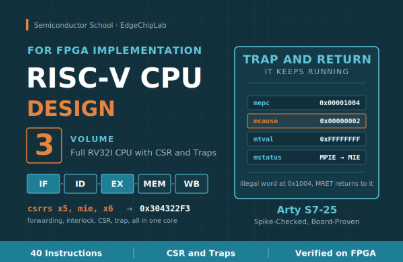
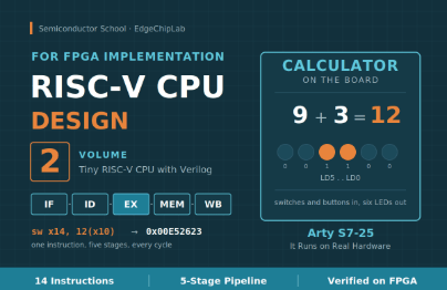
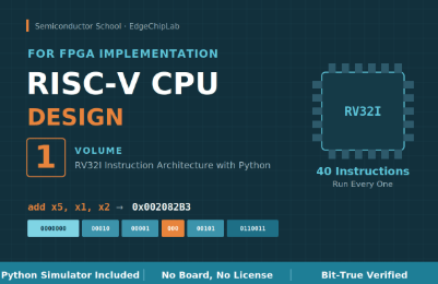
Publications: RISC-V RV32I: From Fundamentals to FPGA Implementation and other semiconductor and digital design educational content. (Multiple Amazon bestsellers)

The starting point for understanding the semiconductor industry goes beyond knowing the names of companies—it is about understanding what technical problems engineers actually solve. This course provides the complete map.

Recommended for
these people

Who is this course right for?

  • University students majoring in electrical and electronic engineering, computer science, mechanical engineering, materials science, chemistry, physics, or industrial engineering who are preparing for employment in the semiconductor industry

  • A job seeker preparing for employment who wants to understand specific engineering roles and responsibilities at semiconductor companies

  • Learners seeking to establish a career direction in the semiconductor field and create a practical skills-based learning plan

Need to know before starting?

  • Basic interest in the semiconductor industry and willingness to pursue employment

  • Basic knowledge of STEM majors or learning experience in a related field

  • A proactive attitude toward reading and analyzing corporate job postings and job descriptions

Hello
This is EdgeChipLab

Career Verified

Design and implement AI semiconductors directly on FPGAs

As a current university professor, I have incorporated 30 years of experience in the system semiconductor industry and expertise in AI semiconductor research and education.

This is a practical curriculum directly designed and verified on an FPGA by a professor who began as a systems semiconductor researcher in Samsung Electronics’ DS Division, went on to serve as a Director at Samsung’s UK and Germany subsidiaries, and later led the System LSI marketing and sales group before becoming a professor teaching semiconductor engineering.

This is not simply a course on how to use FPGAs.
It is designed to help you understand AI algorithms → directly design NPUs and CPUs in RTL → implement them on an FPGA → verify them on actual hardware → and ultimately expand to AI SoCs.

AI Algorithm → RTL Design → FPGA Implementation → Bit-True Verification → AI SoC


Beyond theory to real-world AI hardware implementation

It is difficult to develop system-level AI semiconductor design capabilities with only scattered, fragmented knowledge.

Learners do not stop at using completed black-box IP. The goal is to progressively develop the system design skills to design AI NPUs and RISC-V CPUs themselves, integrate memory and peripherals, and ultimately build their own AI SoC.

Starting with the fundamentals of transistors and digital circuits, you will progress through FPGAs, CPUs, and NPUs to hardware for accelerating Transformers and LLMs.


We validate the research results on actual FPGA hardware.

This is not a lecture you only watch. Rather than stopping at theory or simple simulations, you will run AI semiconductor circuits you designed yourself on an actual FPGA and perform Bit-True verification, confirming that the Python model and RTL results match down to the last bit.

We also connect the instructor’s research results, including four KCI-indexed papers on AI semiconductors, FPGAs, and RISC-V, with the educational content, applying technologies validated through research to actual design and FPGA implementation.

We provide source code essential for hands-on practice, including our self-developed RISC-V CPU, Python code for image training, and Verilog RTL.

Centered around the affordable Arty S7-25 FPGA board and the free Vivado design tool, this course is designed to allow learners to reproduce the entire process of designing, implementing, and verifying their own work.

It can also be used with Digilent FPGA boards, including the Zybo Z7. You just need to modify the XDC pin mapping (board) and clock division parameters (RTL) to match the board.

The “MNIST NPU with FPGA” course only requires modifying the XDC pin mapping, while the courses using the OLED and Camera require modifying the clock division parameters (RTL).

→The course exercises are configured with clock division parameters based on Arty S7’s 100 MHz input clock. Since other boards have different input clocks (for example, Zybo Z7 has 125 MHz), you will need to recalculate the division values so that the target frequency remains the same. If you miss this point, the display or video may not output properly, which can easily be mistaken for a code error, so please check this.


A seamless full-stack roadmap: from the basics to a mini LLM accelerator

Every lecture is not an isolated fragment, but part of a journey toward completing one vast system.

  • Step 1: AI Theory and Image Processing Fundamentals (including Machine Learning)

  • Step 2: AI Accelerator (NPU) Design and Verification (Including Machine Learning)

  • Step 3: RISC-V CPU Design and System Integration

  • Step 4: Advanced AI SoC Implementation and Expansion into a mini LLM Acceleration Platform (Continuous Content Updates)


Objective verification metrics

All design deliverables from this course have undergone rigorous validation against global standards and by the academic community.

  • RISC-V Architecture Verification: In-house developed RISC-V CPU, passed the International Foundation’s official compliance test (ACT), and source code released (GitHub)

  • Academic Authority: Four Sole-Author Academic Papers (published in the prestigious KCI A-ranked journal IJIBC)

  • Global Recognition: Published four global Amazon technology books (reached #1 bestseller status)


    Published books: Roger Kim: books, biography, latest update

  • Real-World Operation Verification Complete: Core IPs, including the RV32I CPU, NPU, vision system, GPS, Transformer, and AURA-Edge SoC, operate flawlessly in the Arty S7 environment.


Take on the challenge. By the time you complete this process of uploading code to the board yourself and checking the results, you will have leveled up into a hardware engineer with a completely different perspective than before.

More

Curriculum

All

4 lectures ∙ (1hr 28min)

Course Materials:

Lecture resources
Published: 
Last updated: 

Reviews

Not enough reviews.
Please write a valuable review that helps everyone!

EdgeChipLab's other courses

Check out other courses by the instructor!

Similar courses

Explore other courses in the same field!

Limited time deal

$20,790.00

30%

$23.10