inflearn logo

Complete Theory of RISC-V CPU Design | From RV32I Instructions to a 5-Stage Pipeline and Hazards

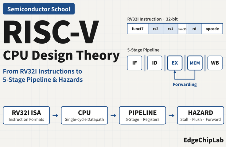
Systematically learn everything from the RISC-V RV32I instruction set to the internal architecture of a 5-stage pipelined CPU. Analyze the operating principles of the datapath, control signals, and pipeline registers, as well as hazard-handling mechanisms such as forwarding, stalls, and flushes, cycle by cycle, to build a solid theoretical foundation for Verilog RTL design and FPGA implementation.

1 learners are taking this course

Level Intermediate

Course period Unlimited

Architecture
Architecture
cpu
cpu
riscv
riscv
system-design
system-design
risk-analysis
risk-analysis
Architecture
Architecture
cpu
cpu
riscv
riscv
system-design
system-design
risk-analysis
risk-analysis

What you will gain after the course

  • Design Principles for the Datapath and Control Architecture of an RV32I Instruction Format and Five-Stage Pipeline CPU

  • Data Transfer Through Pipeline Registers and Hazard Handling Mechanisms: Forwarding, Stalling, and Flushing

  • How CPU Microarchitecture Works: An Analysis of Cycle-by-Cycle Instruction Execution

Master the Theory of RISC-V CPU Design

From RV32I instructions to the 5-stage pipeline and hazards

How does a CPU execute instructions?

Knowing RISC-V instructions does not mean you understand how a CPU works internally.

When executing a single ADD instruction, where does the CPU read the data from, which circuit performs the operation, and where is the result stored?

What happens in a pipelined CPU, where multiple instructions execute simultaneously, if a subsequent instruction needs the result of a previous instruction before it has been stored in a register?

This course starts with this question.

A free theory course that explains how CPU hardware works step by step, from the RISC-V RV32I instruction structure to the CPU datapath, 5-stage pipeline, forwarding, stalls, and flushes.

Rather than simply memorizing instruction types or introducing CPU block names, the goal is to understand how instructions execute, focusing on the Datapath and Control structures used in actual CPU design.


What you will learn

SECTION 1. RISC-V RV32I Instruction Structure and CPU Execution Principles

Understand ISA (Instruction Set Architecture), the starting point of CPU design.

We explore the basic concepts of RISC-V and RV32I, register structure, instruction formats and encoding, and explain what operations instructions require of the CPU hardware.

  • The Difference Between RISC-V ISA and Microarchitecture

  • RV32I Registers and Instruction Formats

  • R-type, I-type, S-type, B-type, U-type, J-type

  • Opcode and Immediate Encoding

  • Arithmetic operations, Load/Store, Branch, and Jump

  • Register File, ALU, Datapath, and Control Unit

  • Basic Execution Principle of a Single-Cycle CPU

SECTION 2. RV32I 5-Stage Pipelined CPU and Datapath Design

We extend from the basic structure that processes instructions sequentially to a pipeline architecture that executes multiple instructions concurrently.

Using the Datapath of an actual 5-stage Pipeline CPU as a reference, we examine the role of each stage and how data and control signals are passed through the Pipeline Registers.

  • Differences Between Single-Cycle CPUs and Pipeline CPUs

  • IF (Instruction Fetch)

  • ID(Instruction Decode)

  • EX (Execute)

  • MEM(Memory Access)

  • WB (Write-back)

  • IF/ID, ID/EX, EX/MEM, MEM/WB Pipeline Register

  • ALU Datapath and Write-back Path

  • Generation and Transmission of Control Signals

SECTION 3. Pipeline Hazards and Instruction Execution Analysis

In a pipeline CPU, multiple instructions proceed simultaneously, which leads to data dependencies and branch-handling problems.

This lecture explains the principles of Forwarding, Stall, Bubble, and Flush for solving these problems, and analyzes hardware behavior by walking through the cycle-by-cycle execution of an example program.

  • Data Hazards and RAW (Read After Write) Dependencies

  • Forwarding Unit and ForwardA/ForwardB

  • EX/MEM and MEM/WB Forwarding

  • Forwarding Priority

  • Register File Write-through

  • Load-use Hazard and Stall

  • 파이프라인 버블

  • Branch, Jump, and Pipeline Flush

  • Cycle-by-Cycle Instruction Execution Analysis

  • A comprehensive example of multiple instructions executing concurrently.


Course Features

1. Learn everything as one continuous journey, from ISA to pipelining.

First, we understand the instruction structure, then examine the CPU datapath that executes those instructions, and finally connect this to the problems that arise when multiple instructions execute simultaneously and how to solve them.

2. Explanations focus on the actual CPU hardware architecture.

Rather than stopping at abstract computer architecture concepts, we analyze the roles of the Register File, ALU, Multiplexer, Pipeline Register, Forwarding Unit, and Hazard Detection Unit, and how they are connected.

3. Clearly distinguish between Forwarding, Stall, and Flush.

Forwarding is a way to pass a result directly, Stall is a way to temporarily halt instruction progress, and Flush is a way to invalidate instructions on an incorrect execution path.

Explain when each function is needed and how it works, with examples.

4. Verify Pipeline behavior with cycle-by-cycle execution logs.

Analyze cycle by cycle how instructions pass through IF, ID, EX, MEM, and WB.

In particular, we examine how instructions with data dependencies, Load-use Stalls, Branch Flushes, and other factors affect the actual Pipeline execution.

5. Leads to hands-on CPU design practice.

This course is a theoretical introduction to understanding CPU architecture and how it works.

Afterward, you can expand your learning to Python-based instruction execution, Verilog RTL design, Testbench simulation, and FPGA implementation.


What will I be able to do after taking this course?

By the end of the course, you will be able to:

  • You will be able to explain the structure of RV32I instructions and how they execute.

  • You will be able to analyze the paths data takes through the CPU datapath.

  • Can distinguish each stage of the 5-Stage Pipeline and the role of the Pipeline Registers.

  • Can determine which value the Forwarding Unit should select.

  • Can explain why a stall is needed for a load-use hazard.

  • You can understand how Pipeline Flush operates with Branch and Jump instructions.

  • You can track the execution of multiple instructions cycle by cycle.

  • You can develop the architectural fundamentals needed to study hands-on CPU design using Verilog.


Recommended for these learners

  • University students who want to learn RISC-V and CPU architecture systematically from the ground up.

  • Learners who want to build on their study of digital logic circuits and move into CPU design

  • Those who want to understand computer architecture theory by connecting it to how real circuits operate.

  • Those preparing to design CPU RTL using Verilog HDL.

  • Engineers interested in implementing an FPGA-based RISC-V CPU

  • Those who want to fully understand how pipeline hazards, forwarding, stalls, and flushes work.

It will be easier to follow if you understand digital logic circuits and basic concepts such as registers, ALUs, and multiplexers.


Course Structure and Learning Materials

This course consists of 3 sections and 3 videos.

  • Section 1: RISC-V Fundamentals & CPU Implementation — Book 1

  • Section 2: RV32I 5-Stage Pipeline CPU Design — Book 2, Part 1

  • Section 3: RV32I 5-Stage Pipeline CPU Design — Book 2, Part 2

The course focuses on understanding the theory, using technical diagrams and execution examples.

This course does not include hands-on practice writing Verilog RTL or implementing designs on an FPGA board. These topics are covered in a follow-up hands-on course.


Next step: Try designing a RISC-V CPU yourself

Once you understand how a CPU works, the next step is to design one yourself.

Semiconductor School’s Inflearn hands-on course is structured as follows.

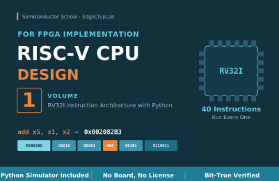
① RISC-V CPU Design for FPGA Implementation — Learn the Structure and Execution of RV32I Instructions with Python

This course uses Python to teach the structure and execution process of RV32I instructions.

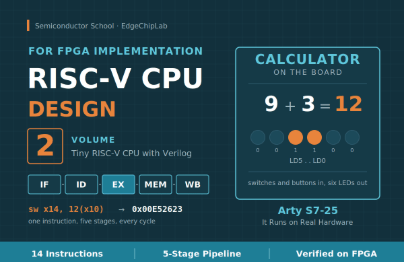
② Designing a RISC-V CPU for FPGA Implementation — Build Your Own 5-Stage Pipeline TinyRV32I

A course on designing a 5-stage pipeline CPU with Verilog HDL and extending it through simulation and FPGA implementation.

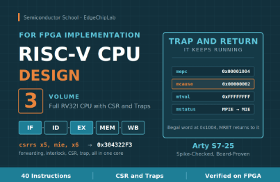
③ RISC-V CPU Design for FPGA Implementation — Build a Full CPU Supporting All 40 RV32I Instructions

An advanced course in designing and verifying a CPU that supports all 40 RV32I instructions.

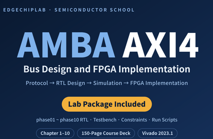
You can then broaden your learning from CPU design to bus interfaces and system integration through the course “AMBA AXI4 Bus Design and FPGA Implementation — From RTL to System Integration.”

RISC-V ISA → CPU Architecture → RTL Design → Simulation → FPGA Implementation → System Integration


About the Knowledge Sharer

Roger Kim | Semiconductor School

I worked in the Semiconductor Division of Samsung Electronics’ Device Solutions (DS) division for about 30 years. I currently teach courses on semiconductors and digital hardware design in the Department of Next-Generation Semiconductor Engineering at Soongsil University.

I create educational content focused on RISC-V CPUs, FPGAs, AI NPUs, AMBA AXI4 buses, and SoC design, connecting the principles of hardware operation with practical implementation and verification.

Book: RISC-V RV32I: From Fundamentals to FPGA Implementation (published on Amazon)

Semiconductor School — Learn the Architecture. Build the Hardware.

Recommended for
these people

Who is this course right for?

  • A computer engineering undergraduate student just beginning a RISC-V-based CPU design project

  • A learner preparing to implement a CPU on an FPGA after studying digital logic circuits and Verilog HDL.

  • An embedded engineer seeking to connect computer architecture theory with practical hardware design.

Need to know before starting?

  • Fundamentals of Digital Logic Circuits (Combinational Circuits, Sequential Circuits, Registers)

  • Basic Computer Architecture Concepts (Instructions, Registers, Memory, ALU)

  • Interest in and willingness to learn hardware description languages (HDLs) or CPU design

Hello
This is EdgeChipLab

Career Verified

"In the AI era, the surest response is to build AI semiconductors yourself."

This program is neither a theory-focused university course nor the standardized curriculum of a contract department tailored to specific specifications. Nor is it limited to simply gaining experience using EDA tools or leveraging libraries, as in conventional fragmented practical seminars.

It is a one-of-a-kind, hands-on course designed and FPGA-validated by a practicing engineering professor with 30 years of experience, who began as a systems semiconductor researcher in Samsung Electronics’ DS Division, won the Silver Prize (Group Chairman’s Award) at the Samsung Technology Awards in the field of design automation, and went on to serve as a Director at Samsung’s UK and German subsidiaries and as the head of the System LSI Marketing and Sales Group.

[ Key differentiators for working professionals & aspiring engineers ]

  • Overcome the limitations of working engineers: Go beyond simply modifying code or using off-the-shelf IP to acquire practical, architecture-level expertise in designing NPUs and CPUs directly in RTL.

  • Establishing a Full-Flow practical system: Complete the entire value chain, from analyzing AI algorithms to FPGA implementation and Bit-True hardware integration verification, and extending to an AI SoC based on a CPU + NPU + RTOS.

  • Field validation complete: Going beyond theory taught in university classrooms, we deliver proven processes that can be applied immediately in real-world work, distilling design expertise from the front lines of industry.

AI Algorithm → RTL Design → FPGA Implementation → Bit-True Verification → AI SoC

For undergraduates and graduate students, as well as working professionals seeking to advance as next-generation AI semiconductor/SoC designers, it provides an unparalleled, top-tier practical guide.


Beyond theory to actual AI hardware implementation

It is difficult to develop system-level AI semiconductor design capabilities with only scattered, fragmented knowledge.

Students do not stop at using completed black-box IP. The goal is to progressively develop the system design skills needed to design an AI NPU and RISC-V CPU themselves, integrate memory and peripherals, port an RTOS on top of them, and ultimately build their own AI SoC.

Starting with the fundamentals of transistors and digital circuits, this course connects FPGA, CPU, and NPU technologies to hardware for accelerating Transformers and LLMs.


We validate the research results on actual FPGA hardware.

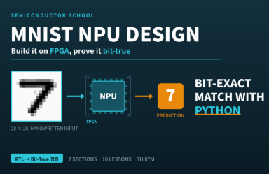
This is not a lecture you only watch. Rather than stopping at theory or simple simulations, you will run AI semiconductor circuits you designed yourself on an actual FPGA and perform Bit-True verification, confirming that the Python model and RTL results match down to the last bit.

The instructor also connects research results, including four KCI-indexed papers on AI semiconductors, FPGAs, and RISC-V, to the educational content, taking technologies validated through research into actual design and FPGA implementation. The source code needed for the exercises—including a self-developed RISC-V CPU, Python code for image training, and Verilog RTL—is made available.

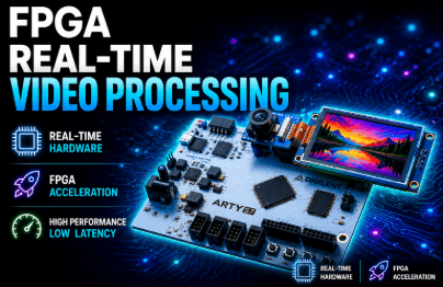
Built around the affordable Arty S7-25 FPGA board and the free Vivado design tool, this course enables learners to reproduce the entire process of designing, implementing, and verifying their own work. It can also be used with Digilent FPGA boards, including the Zybo Z7. Simply modify the XDC pin mapping (board) and clock division parameters (RTL) to match your board. The 'MNIST NPU with FPGA' course only requires modifying the XDC pin mapping, while courses that use an OLED and camera require modifying the clock division parameters (RTL).

→The lecture exercises are configured with divider parameters based on Arty S7’s 100 MHz input clock. Since other boards have different input clocks (e.g., Zybo Z7 uses 125 MHz), you will need to recalculate the divider values so that the target frequency remains the same. If you overlook this, the screen or video may not display properly,so please check, as it can easily be mistaken for a code error.


A seamless full-stack roadmap: from the basics to a mini LLM accelerator

Every lecture is not an isolated fragment, but part of a journey toward completing one vast system.

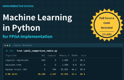
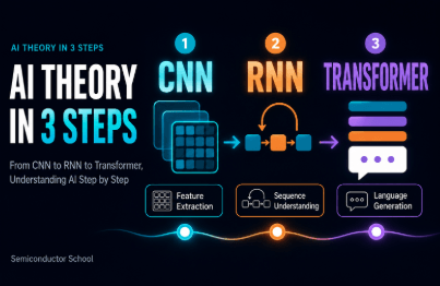
  • Step 1: AI Theory and Image Processing Fundamentals (including Machine Learning)

  • Step 2: AI Accelerator (NPU) Design and Verification (Including Machine Learning)

  • Step 3: RISC-V CPU Design and System Integration

  • Step 4: Advanced AI SoC Implementation and Expansion into a mini LLM Acceleration Platform (Continuous Content Updates)


Objective verification metrics

All design deliverables from this course have undergone rigorous validation against global standards and by the academic community.

  • RISC-V Architecture Verification: In-house developed RISC-V CPU, passed the International Foundation’s official compliance test (ACT), and source code released (GitHub)

  • Academic Authority: Four Sole-Author Academic Papers (published in the prestigious KCI A-ranked journal IJIBC)

  • Global Recognition: Published four global Amazon technology books (reached #1 bestseller status)


    Published books: Roger Kim: books, biography, latest update

  • Real-World Operation Verification Complete: Core IPs, including the RV32I CPU, NPU, vision system, GPS, Transformer, and AURA-Edge SoC, operate flawlessly in the Arty S7 environment.


Take on the challenge. By the time you complete this process of uploading code to the board yourself and checking the results, you will have leveled up into a hardware engineer with a completely different perspective than before.

More

Curriculum

All

3 lectures ∙ (2hr 37min)

Published: 
Last updated: 

Reviews

Not enough reviews.
Please write a valuable review that helps everyone!

EdgeChipLab's other courses

Check out other courses by the instructor!

Similar courses

Explore other courses in the same field!

Limited time deal

$409,295.00

29%

$22.00