

RISC-V CPU Design for FPGA Implementation ③ Building a Full CPU with All 40 RV32I Instructions from Scratch
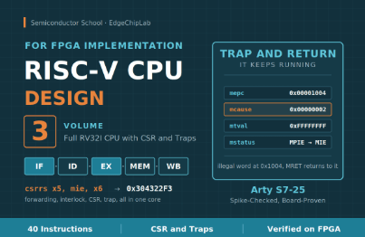
As you study CPUs and RISC-V, you may understand what the instructions do but still find yourself asking, “How are these instructions actually executed in hardware?” and “How can I verify that a CPU I designed myself really works correctly?” Many existing resources stop at ISA explanations or simple CPU examples, and many others rely on completed IP, making it difficult to experience the entire process of designing and verifying a CPU yourself and running programs on an actual FPGA. I have spent many years working in R&D and business in the system semiconductor field, and I have observed this learning gap firsthand while teaching semiconductor design and FPGA at a university. For this reason, rather than providing a completed CPU and simply checking that it operates, this course is structured around designing the CPU directly in a White Box approach, starting with the question, “What hardware is required to execute RV32I instructions?” In Volume 3, we expand Volume 2’s TinyRV32I into a Full-Version 32-bit CPU that uses 40 RV32I instructions. We extend the datapath, Decoder, Branch·Jump, and Byte/Halfword Memory Access, and implement Forwarding and Load-Use Interlock so that the 5-stage Pipeline can handle data dependencies on its own. We then integrate CSR, Exception, Interrupt, Trap, and MRET to complete a CPU capable of handling not only normal program execution but also exceptions and external events. The design does not end with RTL Simulation. You will run actual programs on the CPU, compare the results with the Spike Reference Model, and learn the purpose of the RISC-V Architecture Compatibility Test as well as how to perform and evaluate it through real verification cases. Finally, you will implement the verified CPU on an Arty S7-25 FPGA, receive input from Switches and Buttons, run programs, and confirm the results by displaying them on LEDs. The problem this course aims to solve is not simply learning more RISC-V instructions. Its goal is to connect instructions → CPU architecture → Verilog RTL → Pipeline control → program execution → standards-based verification → actual FPGA operation into a single flow, enabling students to fundamentally understand the internal structure of a CPU and develop the engineering skills to design and verify one themselves.
3 learners are taking this course
Level Intermediate
Course period Unlimited
News
