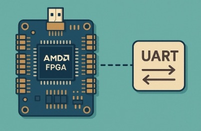
강의

멘토링

커뮤니티

Hardware

/

Semiconductor

Fundamentals of FPGA

In this lecture, we will understand the basic concepts and operating principles of FPGAs, and examine the advantages of FPGAs and their differences from ASICs. Next, we will explain the FPGA design process and detailed FPGA design areas. We will learn about the types and roles of FPGA development tools, and proceed with the installation of Vivado, an AMD FPGA development tool. Through a simple example design practical exercise, you will experience the FPGA design process.

(4.6) 26 reviews

453 learners

Level Beginner

Course period 6 months

  • EasyFPGA
Verilog HDL
Verilog HDL
FPGA
FPGA
system-verilog
system-verilog
Verilog HDL
Verilog HDL
FPGA
FPGA
system-verilog
system-verilog
Thumbnail

Reviews from Early Learners

Reviews from Early Learners

4.6

5.0

배부한

100% enrolled

It was very helpful to have FPGA coding explained in an easy and simple way, including how it works and what internal structure it operates with.

5.0

haneuli

25% enrolled

It helped me understand FPGA architecture a lot. Thank you.

5.0

dmax

100% enrolled

This was a new learning experience. Thank you.

What you will gain after the course

  • Understanding FPGA's Definition and Operating Principles

  • Identifying the value of FPGA utilization through a comparison of FPGA and ASIC

  • Familiarity with FPGA design process (HDL coding → synthesis → place and route → bitstream generation)

  • Identifying required technologies in FPGA detailed design areas (interface, algorithm, and parallel processing)

  • Understanding FPGA Development Tools

  • Understanding the installation methods for AMD FPGA development tools, Vivado and Vitis

  • Vivado Development Flow Using Example Designs

FPGA Image

Introduction to the course

This course covers the basic concepts of the structure and design flow of FPGAs (Field-Programmable Gate Arrays) , and covers the two axes of interface design and algorithm design that constitute the design from a practical perspective. This is an introductory course for those who want to systematically learn FPGA design, from beginners to practitioners.

Also, FPGA design is essentially similar to the front-end process of ASIC design. Therefore, it is a good preparation process for entering ASIC design . In fact, it is common to perform prototyping with FPGA at the beginning of an ASIC project, and this common ground is also why there are many engineers who are skilled in both ASIC and FPGA.

Learning Objectives

  • Understand what FPGAs are and why they are used.

  • Learn the FPGA design flow step by step.

  • Identify key elements of interface design (clocks, I/O, memory, high-speed communications, etc.).

  • Understand the concepts of designing algorithms and parallel processing structures (DSP, LUT, pipelining, FSM, etc.).

  • Understand how to configure the system in an integrated manner and what to watch out for.

  • Understand FPGA development tools and learn how to install AMD FPGA development tools.

  • Learn how to use FPGA internal components such as CLB, memory blocks, and DSP.

What is an FPGA?

FPGA (Field Programmable Gate Array) is an abbreviation for "field programmable gate array" and is a semiconductor chip that allows users to freely configure the hardware circuit structure.

  • Reconfigurability: the ability to reprogram hardware circuits to suit the desired behavior.

  • Applications: Communication, signal processing, artificial intelligence, robot control, high-speed interface, etc.

  • Components: Logic Block, LUT, Flip-Flop, Clock Network, Block RAM, DSP Slice, etc.

FPGA Design Flow

  1. Requirements definition

    • Clearly define the functions, performance, and input/output conditions to be implemented

  2. RTL design

    • Design in a hardware description language such as Verilog HDL, system-verilog, or VHDL

  3. Functional Simulation

    • Verify that the design logic meets requirements through simulation

  4. Synthesis

    • Convert RTL code into actual gate-level circuits

  5. Place & Route

    • Design placement on FPGA's actual resources (LUT, FF, DSP, etc.)

  6. Bitstream Generation

    • Generating configuration data that the FPGA can recognize

  7. Programming and Debugging


    • Download to FPGA, check operation, modify if necessary

FPGA Design Subfields

  1. Interface design

    • Understanding of input/output I/O and buffers, clock structures, Gigabit Transceiver, and Memory Interface is required.


  2. Algorithm and Parallel Processing Design

    • DSP utilization, Custom Logic design, FSM design

    • Pipelining and parallel processing design are key.

FPGA Design Tools

  1. Design tools from major device manufacturers

    1. AMD FPGA: Vivado, Vitis

    2. Intel FPGA: Quartus

  2. Key Features

    1. HDL code writing/simulation/synthesis

    2. Setting design constraints (XDC, SDC, etc.)

    3. Timing Analysis and Bitstream Generation

    4. On-chip Debugging

  3. Vivado + Vitis Workflow

    1. Vivado: Hardware Design

    2. Vitis: Software Design


Installing Vivado

  1. Vivado and Vitis are the basic tools required for AMD FPGA development.

  2. You need to create an account on the AMD Site and download the version you want.

    1. The Standard version is free to use, but support for some devices is limited.

    2. The larger the logic size of the device, the larger the memory capacity required for the PC.

  3. installation

    1. Requires 100GB or more of hard disk space.

    2. It takes 1~2 hours or more.

LED Blinking (Example)

  1. Using system-verilog, clock division, and RTL, design an LED that toggles at 1-second intervals.

  2. Create a test bench and run the simulation.

  3. Specify constraints in the XDC file.

  4. Synthesis and Implementation in progress.

  5. Add debugging signals to ILA.

  6. FPGA programming and testing.

FPGA Internal Components

  1. CLB (Configurable Logic Blocks)

  2. Memory

  3. DSP

Recommended for
these people

Who is this course right for?

  • Those interested in FPGA design

  • Those curious about FPGA

  • Those who dream of semiconductor design

Hello
This is

514

Learners

30

Reviews

4

Answers

4.4

Rating

3

Courses

  • Unlike traditional semiconductor design processes, FPGA is a device with the advantage of being able to implement designs quickly and easily. As long as you have the design source, it can be immediately placed and routed using the FPGA's logic elements. Furthermore, due to its strong hardware nature, the code is not complex and can be written intuitively.

  • The important thing is to understand FPGA design concepts and flows, and furthermore, to understand the design objectives and targets. Based on this, the core is to optimize the structure of the design source and input appropriate constraints to design a stable FPGA.

  • The course focuses on FPGA design concepts, architecture, methodologies, and flows rather than just coding, featuring step-by-step, hands-on practice. Building know-how through direct implementation and practical experience is the core of being an FPGA engineer, and this will hold greater value than coding, which is increasingly being replaced by AI.

  • An FPGA and hardware design expert with 10+ years of experience, specializing in high-speed data processing, communication system design, and image processing, with extensive participation in various FPGA projects.

  • You can find additional information on the YouTube channel or blog below.

Specializing in areas such as [these], I have participated in various FPGA projects. You can find more information on the YouTube channel or blog below. https://www.youtube.com/@easy-fpga easyfpga.blog

Specializing in areas such as [this/these], I have participated in various FPGA projects. You can find additional information on the YouTube channel or blog below. https://www.youtube.com/@easy-fpga easyfpga.blog

Curriculum

All

16 lectures ∙ (1hr 39min)

Course Materials:

Lecture resources
Published: 
Last updated: 

Reviews

All

26 reviews

4.6

26 reviews

  • jeruel119219님의 프로필 이미지
    jeruel119219

    Reviews 1

    Average Rating 5.0

    5

    100% enrolled

    It was very helpful to have FPGA coding explained in an easy and simple way, including how it works and what internal structure it operates with.

    • deokryul님의 프로필 이미지
      deokryul

      Reviews 2

      Average Rating 5.0

      5

      31% enrolled

      • neulha님의 프로필 이미지
        neulha

        Reviews 15

        Average Rating 5.0

        Edited

        5

        25% enrolled

        It helped me understand FPGA architecture a lot. Thank you.

        • sirochiri님의 프로필 이미지
          sirochiri

          Reviews 5

          Average Rating 5.0

          5

          63% enrolled

          • ninety25296님의 프로필 이미지
            ninety25296

            Reviews 145

            Average Rating 5.0

            5

            100% enrolled

            This was a new learning experience. Thank you.

            Free

            EasyFPGA's other courses

            Check out other courses by the instructor!

            Similar courses

            Explore other courses in the same field!