Practical PCB Hardware Design: Mixed-Signal Board Design Project Using STM32
The key to competitiveness in circuit design is, ultimately, broad domain experience! Master all the essential hardware knowledge and experience—from STM32 MCUs, Ethernet PHYs, motor drivers, ADCs/DACs, EMI, and ESD—in one place!
707 learners
Level Intermediate
Course period Unlimited
News
4 articles
Hello, this is Sam Coach.
I'm writing this because I have some news I'd like to share first with those who have taken the course.
View the Analog Circuit Design Fundamentals Training
It started in the Q&A forum.
Since uploading the lecture, I have been replying to the posts you left on the questions board.
I only increased L, but the gain isn’t what I expected.
The slew rate is coming out absurdly large.
The PSRR is less than 10 dB.
How do you determine the specifications initially?
I could have written down the cause in a reply. But I always felt something was missing while writing it.
To understand why that number came out, I need to run the circuit again and verify it with my own eyes, but I couldn’t provide that experience in a reply.
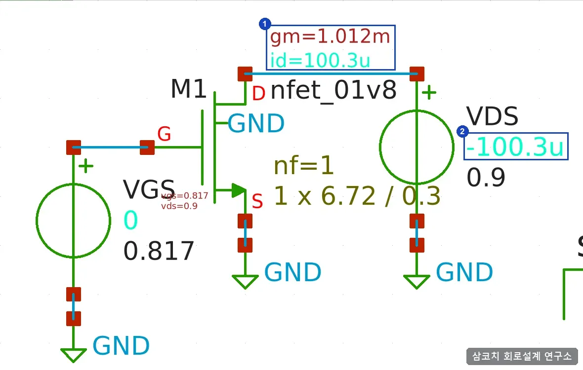
Lab 1 · This is a screen showing the operating point run in xschem displayed directly on the schematic. Read gm and id on the circuit instead of transferring them to a table.
It was the same when designing analog IP at the company. If the hand-calculated values differed from the simulation results, we did not move on to the next step until we found out where the difference came from.
Before moving past a block, I ran both corners and Monte Carlo to fill out the spec table, and a colleague reran the table. In the lecture, I showed you this process on my screen, but it’s something you need to try a few times yourself to get used to.
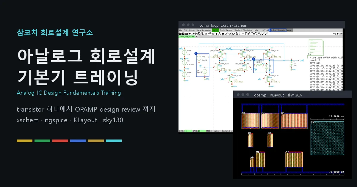
So this time, instead of using my screen, I created a hands-on exercise that you can run on your own PC. It is analog circuit design fundamentals training.
How is it different from the lectures?
In the lectures so far, we mainly used LTspice with the TSMC 180 nm library. In this lab, we switched to xschem, ngspice, and sky130.
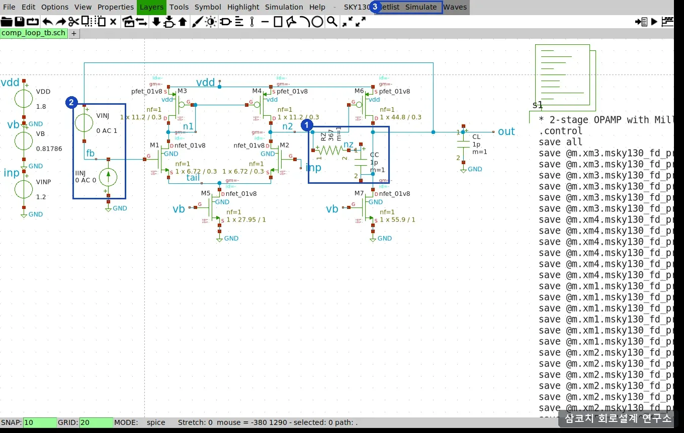
This is the screen showing the Lab 15 · 2-stage OPAMP loop testbench opened in xschem. It was drawn using sky130’s nfet_01v8 · pfet_01v8.
They are all open source, so anyone can install them without a license. sky130 is a PDK for an actual process that has been made public, so it includes corner models and Monte Carlo models, and it also has design rules, allowing you to view the layout at its actual size.
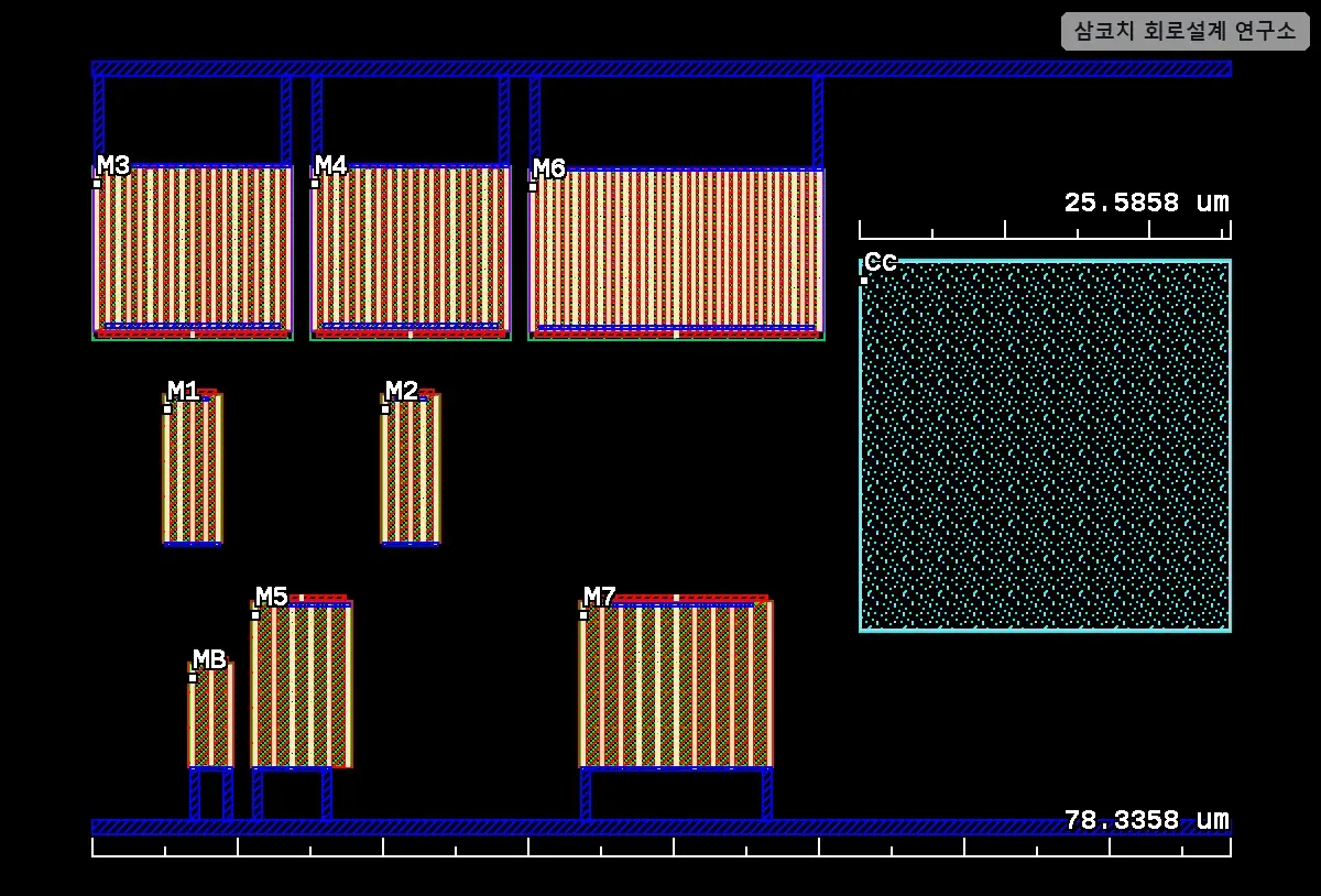
This is a KLayout screen showing the same OPAMP drawn according to the sky130 design rules. The large rectangle on the right is the compensation capacitor Cc.
I also run the 45 corners and Monte Carlo on my PC.
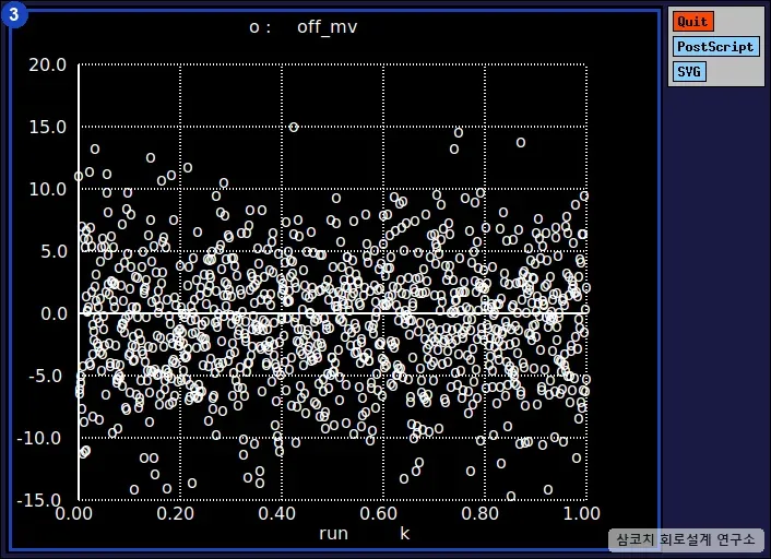
Lab 17 · This is an ngspice screen showing 1,000 Monte Carlo runs of the offset caused by mismatch in the input pair. Each dot represents one run.
For those who will be using Virtuoso · ADE at a company, I have also included a guide showing side by side where to perform the same tasks in Cadence.
A lab proceeds as follows.
The sequence is the same for every lab. First, predict and write down the result, then run it, and see how accurate your prediction was.
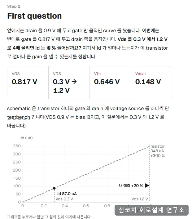
This is the first question in Lab 1. If Vds is increased fourfold from 0.3 V to 1.2 V, by what percentage will Id increase? Before looking at the answer, write down your number first.
Once a prediction is saved, it cannot be changed. The incorrect number needs to remain so that you’ll look for where you went wrong.
The questions listed above are also included in the lab.
A circuit with only L increased is run again in Lab 5.
What determines the slew rate is covered in Lab 15.
How to write and simulate PSRR is covered in Lab 19.
In the spec, we go through the process of determining W and current from scratch for the first time in Lab 9.
Starting with a single transistor, you will design a CS amp, differential pair, current mirror, and eventually a 2-stage OPAMP. The final step is a design review, where you run through a block handed over by a colleague again according to the checklist. There are four Levels and 23 Labs.
At the end of each Level, there is a Level check. You receive a spec you’ve never seen before, determine W · L · current, and the check script grades each spec item. If you take it again, a new spec appears. It’s designed so that you can’t pass by memorizing the answers.
After completing Level 3, you will move on to a set of Project Prep exercises where you run the blocks used in SAR ADCs, PLLs, and DC-DC converters at the transistor level.
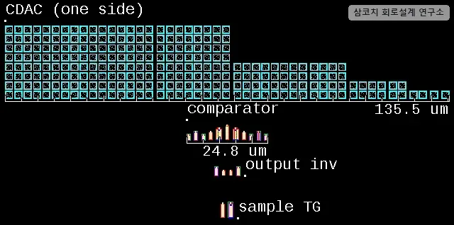
This is the KLayout screen showing the CDAC, comparator, and switch of the SAR ADC core in Project prep 1, drawn according to sky130 design rules.
You can try it for free before making a payment.
The first three screens are free as long as you sign up and log in.
Start check · Install the tools on your PC and check whether the baseline numbers come out correctly.
Lab 1 · Run a transistor and read the operating point on the schematic
Simulation guide · A glossary of ngspice commands and error messages used in the lab
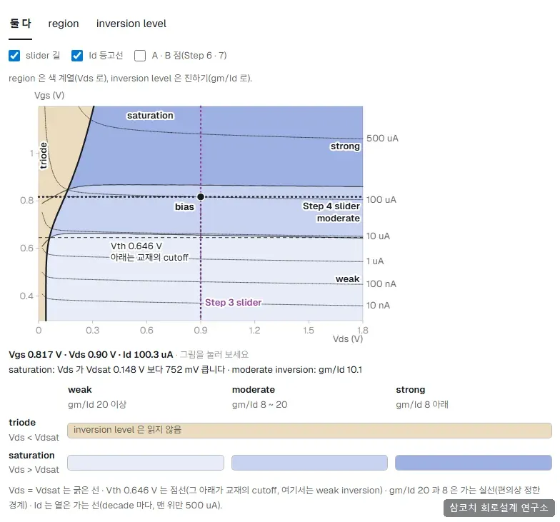
This is a region diagram for Lab 1. It shows on a single page which region the transistor is in according to Vgs and Vds. Lab 1 is free, so you can move this diagram around yourself.
A Windows 10 · 11 PC with at least 30 GB of disk space and 8 GB of memory is required. Check whether it works on your PC first with Start check.
If the tool stops during practice or displays different numbers, please ask through the “Contact Us” link provided at each step. The specific Lab and step will be attached automatically, so you don’t need to explain the situation from the beginning.
You can view the structure and actual screens here.
View the Analog Circuit Design Fundamentals Training
I’m also creating the fundamentals for Digital · Layout · Verification · Implementation · HW board · Embedded in the same way. I’ll let you know again each time one is opened.
Thanks to those who left questions, I was able to understand what I should create as hands-on exercises. Thank you. I’ll continue checking the Q&A board in the future.
Sincerely, Coach Sam
Hello, I'm Samcoach, a circuit design mentor.
These days, AI semiconductors are the hottest keyword in both stocks and industry.
In that trend, the "AI Semiconductor Design Course" I prepared has
finally passed the Ministry of Employment and Labor's government funding review!👉Apply Now
🔹 AI semiconductors become the center of industry
The recent growth rate of the AI industry is beyond imagination.
With the emergence of large language models like GPT, Llama, and Claude,
the computational structure itself across industries is being redefined.At the center of this is the AI semiconductor (AI Accelerator).
No matter how much AI advances,
if the semiconductor architecture responsible for those computations cannot keep up,
speed and efficiency will ultimately hit their limits.So now, the entire world is working to secure AI semiconductor design talent.
Not only Samsung, SK Hynix, NVIDIA, and AMD,
but also domestic startups, fabless companies, and research institutes
are all looking for "people who can structurally design computational efficiency."🔸 After GPU, the era of new architectural competition
In the industry, various design innovations are currently being pursued simultaneously
to overcome the limitations of GPU-based computing.Chiplet Architecture: An approach that designs large chips by dividing them into multiple modules,
reducing manufacturing process constraints and improving heat and yield issues.HBM(High Bandwidth Memory) Integration:
To solve the memory bandwidth bottleneck in AI model training,
technology that directly stacks HBM and minimizes computing units and interfaces is gaining attention.3D Stacking:
A method that vertically stacks logic chips and memory chips to reduce signal delay
in order to achieve much higher computational density than GPUs.
These technologies come together as one,
ultimately converging on "the ability to design efficient computational structures" as the core of AI semiconductors.🔸 Three pillars that circuit designers must master
① Common Practical Skills
Performing RTL design with Verilog/SystemVerilog,
implementing actual circuits through FPGA,
and meeting timing constraints, power, and signal integrity requirements
are fundamental skills for all designers and the 'language of circuits'.
This is no longer optional but essential.② Advanced Specialization in Professional Design Areas
The depth of design varies depending on your career path.
In the power semiconductor field, you'll work on high-efficiency circuit design
such as GaN-based power circuits and
3-level switching chargers,
while in the digital design field, you'll handle
high-speed interface design and verification environment setup for DDR, PCIe, SerDes, etc.
This isn't something you can simply learn - it's an area that can only be understood through direct design and verification.③ Trendy technologies leading the industry
Chiplets, 3D stacking, AI-based EDA,
HBM memory integration, and AI accelerator architecture design.
These five technologies are determining the future of the industry right now.⚙ A course to learn "practical design thinking" rather than theory
To practically connect these three axes,
the "AI Semiconductor Design Practice" course that I personally developed
has been officially approved for the Ministry of Employment and Labor K-Digital Basic Skills Training this time.This course is not simply a "learning lecture."
It is "training to acquire the mindset of a designer."Design arithmetic blocks directly in Verilog and
While implementing CPU architecture
Finally, we add AI computation units to complete the AI accelerator architecture.
The entire course proceeds by constantly asking "Why is this structure efficient?",
"What constraints must be considered in actual chip design?",
"Why is this signal timing set this way?"When you submit assignments, we don't just give you a score,
but also point out actual problems that occur during the Tape-out stage from the perspective of working engineers."This structure may cause Hold Violations."
"While this timing might pass in an FPGA environment, it has a high probability of failing in actual ASIC implementations."This kind of feedback is exactly the moment that creates 'practical design sense'.
👨🏫 Operating Structure and Support System
Operating Platform: COMENTO
Instructor Composition:
Main Instructor 1 person (Semiconductor Circuit Design Engineer from Samsung Electronics S.LSI - Samcoach)
2 Assistant Instructors (Current Circuit Design Engineers)
Support Method:
Real-time Q&A and project-specific feedback
Advanced learning materials, design trend report provided
Operating AI Semiconductor Competition Award-Winning Works Analysis Session
Latest Industry Position Analysis and Career Q&A Session Provided
This system is designed not for simple learning, but
as a structure that leads to practical skills → portfolio building → career expansion.💰 Government funding benefits and completion perks
This course is supported through the Ministry of Employment and Labor's K-Digital Basic Skills Training Program,
with over 90% of tuition fees covered by government funding.
The actual out-of-pocket cost is approximately 42,000 won.Official Certificate of Completion (including NCS code) issued
Lifetime access provided (including updates)
6-month access to Comento Professional Community
→ Technical Q&A and job information sharing available between industry designers and studentsAI Competition Trend Report and Award-Winning Work Analysis Content Provided
AI Semiconductor Employment/Career Change Information Channel Connection Support
This course is originally a hands-on curriculum worth 400,000-500,000 won,
but thanks to government funding, you can take it almost for free.However, due to limited budget,
enrollment closes on a first-come, first-served basis for each cohort.Also, due to the nature of government funding, we don't know when the support will end.
Since the course benefits remain the same,
please don't hesitate and apply when you can.
(It was actually 100% free until 2023, but changed to 90% in 2024.)👉Apply Now
🚀 Expansion After Completion: Career & Competitions
Students who complete this course are not simply "people who learned about AI semiconductors."
They become talent with practical competencies that connect to actual career stages
such as AI semiconductor competitions, design internships, and preparation for employment at semiconductor companies.AI Semiconductor Competition Preparation Class Operation
→ Analysis of actual award-winning structures, providing feedback on submitted circuit designsProviding job search and career transition support content
→ Hiring trends, position analysis, company-specific design capability guidesCommunity Networking
→ Support for study groups, collaborative projects, and information exchange among graduates
In other words, it's not the end of learning but
'a starting point for concretizing your career as an AI semiconductor designer'.The AI semiconductor industry is not simply one field of semiconductors.
It is the center of a new technological ecosystem where AI, systems, and semiconductors converge.
Now, circuit designers are no longer simply "people who design chips,"
but must become "engineers who design AI computational architectures."Through this government-funded program,
develop real industry-level design skills
and grow into a practical talent who can lead the AI semiconductor era.Thank you.
Circuit Design Mentor Samcoach Dream.
(The free resource link was sent incorrectly, so we are sending it again.)
Hello, circuit design job seekers.
Looking at the job market these days,
There is a clear trend of reducing public recruitment and hiring a small number of elite candidates for positions.
Especially for those who have only prepared for digital design, this is a time when they start to worry deeply about whether they are okay going in this direction.I also meet many people in the field and in education.
I often hear people say , 'There is a lot of information, but it is still difficult to find the right direction for me.'So this time,
We have prepared a seminar that will provide you with precise direction and practical preparation methods .This seminar
It's not just a simple transfer of information,
"So that each and every one of you can accurately check your position and draw the next step."
It's designed to provide practical help.✅ Seminar: 2025 Circuit Design Employment Strategy Seminar
👉 Apply for the seminarThe composition is as follows:
Analysis of circuit design job recruitment trends by industry
Importance of Digital+Analog+Verification+System Integration Experience
Sharing real employment/career change success stories
How to increase your practical competitiveness in a short period of time
Free Q&A (All questions regarding employment, job changes, and study directions are welcome)
🎁 Benefits provided to all seminar participants
Free PDF eBook for Circuit Design Entry
20% discount coupon for future classes
(Even if you just attend, we have prepared everything you need to prepare.)
🎯 You will also receive additional materials and special benefits
🔗 [Free Material] Semiconductor Circuit Design Job-Specific Keyword PDF + Recommended Portfolio Guide
→ View directly🎁 [Special benefit for existing students] 30% discount on digital + analog integrated lectures
→ Apply
📢 Additionally, we have prepared a video that we would like you to watch together this time.
2025 Semiconductor Circuit Design Jobs, How to Prepare
Digital design alone is not enough.
Companies are now looking for talent with experience integrating digital and analog.In this video
Vivid insights gained through interviews with recruiters and current employees
Preparation Directions for the 5 Major Circuit Design Jobs
T-shaped talent strategy
How to construct a recommended portfolio
9-month job preparation roadmap
I have summarized everything in detail.
📺 Watch the video now
👉 https://www.youtube.com/watch?v=a8-_rZENV9c(※ Anyone can watch this video for free, regardless of whether or not they have applied for the seminar.)
This seminar
It is not a "preparation that only accumulates information and adds to the frustration",
It was created to help "clear the direction and prepare you to actually move."If you are currently struggling alone,
This seminar will help you find a clear path.Come and join us without any pressure,
Make your circuit design career journey more certain.I sincerely look forward to this time when we can grow together.
thank youSamkochi Dream.
Hello, circuit design job seekers.
Looking at the job market these days,
There is a clear trend of reducing public recruitment and hiring a small number of elite candidates for positions.
Especially for those who have only prepared for digital design, this is a time when they start to worry deeply about whether they are okay going in this direction.I also meet many people in the field and in education.
I often hear people say , 'There is a lot of information out there, but it is still difficult to find the right direction for me.'So this time,
We have prepared a seminar that will provide you with precise direction and practical preparation methods .This seminar
It's not just a simple transfer of information,
"So that each and every one of you can accurately check your position and draw the next step."
It's designed to provide practical help.✅ Seminar: 2025 Circuit Design Employment Strategy Seminar
👉 Apply for the seminarThe composition is as follows:
Analysis of circuit design job recruitment trends by industry
Importance of Digital+Analog+Verification+System Integration Experience
Sharing real employment/career change success stories
How to increase your practical competitiveness in a short period of time
Free Q&A (All questions regarding employment, job changes, and study directions are welcome)
🎁 Benefits provided to all seminar participants
Free PDF eBook for Circuit Design Entry
20% discount coupon for future classes
(Even if you just attend, we have prepared everything you need to prepare.)
🎯 You will also receive additional materials and special benefits
🔗 [Free Material] Semiconductor Circuit Design Job-Specific Keyword PDF + Recommended Portfolio Guide
→ View directly🎁 [Special benefit for existing students] 30% discount on digital + analog integrated lectures
→ Apply
📢 Additionally, we have prepared a video that we would like you to watch together this time.
2025 Semiconductor Circuit Design Jobs, How to Prepare
Digital design alone is not enough.
Companies are now looking for talent with experience integrating digital and analog.In this video
Vivid insights gained through interviews with recruiters and current employees
Preparation Directions for the 5 Major Circuit Design Jobs
T-shaped talent strategy
How to construct a recommended portfolio
9-month job preparation roadmap
I have summarized everything in detail.
📺 Watch the video now
👉 https://www.youtube.com/watch?v=a8-_rZENV9c(※ Anyone can watch this video for free, regardless of whether or not they have applied for the seminar.)
This seminar
It is not a "preparation that only accumulates information and adds to the frustration",
It was created to help "clear the direction and prepare you to actually move."If you are currently struggling alone,
This seminar will help you find a clear path.Come and join us without any pressure,
Make your circuit design career journey more certain.I sincerely look forward to this time when we can grow together.
thank youSamkochi Dream.