강의

멘토링

로드맵

Hardware

/

Semiconductor

Fundamentals of FPGA

In this lecture, we will understand the basic concepts and operating principles of FPGAs, and examine the advantages of FPGAs and their differences from ASICs. Next, we will explain the FPGA design process and detailed FPGA design areas. We will learn about the types and roles of FPGA development tools, and proceed with the installation of Vivado, an AMD FPGA development tool. Through a simple example design practical exercise, you will experience the FPGA design process.

(4.7) 9 reviews

161 learners

  • EasyFPGA
fpga기초
fpga이해
fpga디자인플로우
Verilog HDL
FPGA
system-verilog
Thumbnail

Reviews from Early Learners

What you will learn!

  • Understanding FPGA's Definition and Operating Principles

  • Identifying the value of FPGA utilization through a comparison of FPGA and ASIC

  • Familiarity with FPGA design process (HDL coding → synthesis → place and route → bitstream generation)

  • Identifying required technologies in FPGA detailed design areas (interface, algorithm, and parallel processing)

  • Understanding FPGA Development Tools

  • Understanding the installation methods for AMD FPGA development tools, Vivado and Vitis

  • Vivado Development Flow Using Example Designs

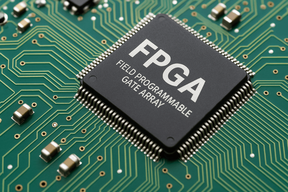
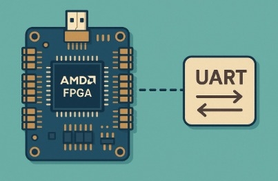
FPGA Image

Introduction to the course

This course covers the basic concepts of the structure and design flow of FPGAs (Field-Programmable Gate Arrays) , and covers the two axes of interface design and algorithm design that constitute the design from a practical perspective. This is an introductory course for those who want to systematically learn FPGA design, from beginners to practitioners.

Also, FPGA design is essentially similar to the front-end process of ASIC design. Therefore, it is a good preparation process for entering ASIC design . In fact, it is common to perform prototyping with FPGA at the beginning of an ASIC project, and this common ground is also why there are many engineers who are skilled in both ASIC and FPGA.

Learning Objectives

  • Understand what FPGAs are and why they are used.

  • Learn the FPGA design flow step by step.

  • Identify key elements of interface design (clocks, I/O, memory, high-speed communications, etc.).

  • Understand the concepts of designing algorithms and parallel processing structures (DSP, LUT, pipelining, FSM, etc.).

  • Understand how to configure the system in an integrated manner and what to watch out for.

  • Understand FPGA development tools and learn how to install AMD FPGA development tools.

  • Learn how to use FPGA internal components such as CLB, memory blocks, and DSP.

What is an FPGA?

FPGA (Field Programmable Gate Array) is an abbreviation for "field programmable gate array" and is a semiconductor chip that allows users to freely configure the hardware circuit structure.

  • Reconfigurability: the ability to reprogram hardware circuits to suit the desired behavior.

  • Applications: Communication, signal processing, artificial intelligence, robot control, high-speed interface, etc.

  • Components: Logic Block, LUT, Flip-Flop, Clock Network, Block RAM, DSP Slice, etc.

FPGA Design Flow

  1. Requirements definition

    • Clearly define the functions, performance, and input/output conditions to be implemented

  2. RTL design

    • Design in a hardware description language such as Verilog HDL, system-verilog, or VHDL

  3. Functional Simulation

    • Verify that the design logic meets requirements through simulation

  4. Synthesis

    • Convert RTL code into actual gate-level circuits

  5. Place & Route

    • Design placement on FPGA's actual resources (LUT, FF, DSP, etc.)

  6. Bitstream Generation

    • Generating configuration data that the FPGA can recognize

  7. Programming and Debugging


    • Download to FPGA, check operation, modify if necessary

FPGA Design Subfields

  1. Interface design

    • Understanding of input/output I/O and buffers, clock structures, Gigabit Transceiver, and Memory Interface is required.


  2. Algorithm and Parallel Processing Design

    • DSP utilization, Custom Logic design, FSM design

    • Pipelining and parallel processing design are key.

FPGA Design Tools

  1. Design tools from major device manufacturers

    1. AMD FPGA: Vivado, Vitis

    2. Intel FPGA: Quartus

  2. Key Features

    1. HDL code writing/simulation/synthesis

    2. Setting design constraints (XDC, SDC, etc.)

    3. Timing Analysis and Bitstream Generation

    4. On-chip Debugging

  3. Vivado + Vitis Workflow

    1. Vivado: Hardware Design

    2. Vitis: Software Design


Installing Vivado

  1. Vivado and Vitis are the basic tools required for AMD FPGA development.

  2. You need to create an account on the AMD Site and download the version you want.

    1. The Standard version is free to use, but support for some devices is limited.

    2. The larger the logic size of the device, the larger the memory capacity required for the PC.

  3. installation

    1. Requires 100GB or more of hard disk space.

    2. It takes 1~2 hours or more.

LED Blinking (Example)

  1. Using system-verilog, clock division, and RTL, design an LED that toggles at 1-second intervals.

  2. Create a test bench and run the simulation.

  3. Specify constraints in the XDC file.

  4. Synthesis and Implementation in progress.

  5. Add debugging signals to ILA.

  6. FPGA programming and testing.

FPGA Internal Components

  1. CLB (Configurable Logic Blocks)

  2. Memory

  3. DSP

Recommended for
these people

Who is this course right for?

  • Those interested in FPGA design

  • Those curious about FPGA

  • Those who dream of semiconductor design

Hello
This is

204

Learners

12

Reviews

3

Answers

4.2

Rating

3

Courses

  • FPGA는 전통적인 반도체 설계 과정과 달리, 쉽고 빠르게 설계를 구현할 수 있는 장점을 가진 디바이스입니다. 디자인 소스만 있으면, FPGA의 논리 요소를 활용하여, 즉시 배치 및 연결이 가능합니다. 또한, 하드웨어적인 성격이 강하기 때문에 코드 역시 복잡하지 않고 직관적으로 작성할 수 있습니다.

  • 중요한 것은 FPGA의 설계 개념과 Flow를 이해하며, 나아가서는 설계 목적과 대상에 대해 이해를 하는 것입니다. 이를 바탕으로 디자인 소스의 구조를 최적화하고, 알맞은 제약조건을 입력해 안정적인 FPGA를 설계하는 것이 핵심입니다.

  • 강의에서는 코딩보다는 FPGA 설계 개념과 구조, 설계 방식 및 Flow를 중심으로 구성되며, Step-by-Step 실습 위주의 내용을 담을 것 입니다. 직접 구현하고 실습하며 노하우를 쌓아가는 것이 FPGA 엔지니어의 핵심이며, 앞으로 AI로 대체될 코딩 보다 더 큰 가치가 될 것입니다.


  • 10+ 경력의 FPGA 및 하드웨어 설계 전문가로, 고속 데이터 처리 및 통신 시스템 설계, 영상 처리 등에 특화되어 있으며, 다양한 FPGA 프로젝트에 참여.

  • 아래 Youtube나 Blog에서 추가적인 정보를 얻으실 수 있습니다.


Curriculum

All

16 lectures ∙ (1hr 39min)

Course Materials:

Lecture resources
Published: 
Last updated: 

Reviews

All

9 reviews

4.7

9 reviews

  • haneuli님의 프로필 이미지
    haneuli

    Reviews 14

    Average Rating 5.0

    Edited

    5

    25% enrolled

    FPGA 구조를 이해하는데 도움이 많이 됐어요. 감사합니다.

    • dmax님의 프로필 이미지
      dmax

      Reviews 121

      Average Rating 5.0

      5

      100% enrolled

      새로운 학습이었습니다. 고맙습니다

      • Jang Jaehoon님의 프로필 이미지
        Jang Jaehoon

        Reviews 558

        Average Rating 4.8

        5

        100% enrolled

        좋은 강의 감사합니댜!

        • SH Chang님의 프로필 이미지
          SH Chang

          Reviews 1

          Average Rating 5.0

          5

          63% enrolled

          • 이석중님의 프로필 이미지
            이석중

            Reviews 1

            Average Rating 3.0

            3

            31% enrolled

            Free

            EasyFPGA's other courses

            Check out other courses by the instructor!

            Similar courses

            Explore other courses in the same field!