Refreshing Gaviscon: A Secret Talk Concert with Gaebalbadak
inflearn

Free
Beginner / career-advice, career, career-development
5.0
(9)
300+

Beginner
career-advice, career, career-development

Through this lecture, you can gain information related to thin film deposition process technology and process development! For process technology and process development engineers, it is important to understand not only the processes but also the equipment. In this lecture, I will introduce the equipment and share my personal work experience. Try to actively incorporate the contents of this lecture into your self-introduction & resume!!
18 learners
Level Basic
Course period Unlimited
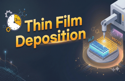
Structure of PECVD Equipment
Introduction to Practical Work
Are there any of you currently preparing for Thin Film process technology or process development roles?!
Don't you find it frustrating when you're looking for study materials and everything is so fragmented?
I also struggled a lot trying to find study materials back when I was preparing for employment ㅠㅠ
At that time, the information was so scattered that it was really difficult to establish a proper direction for my studies.
I was also at a loss as to how theory and actual processes were connected,
As I organized everything one by one, a great opportunity eventually came my way,
I am currently working at a foreign semiconductor company.
And so... I have created a Thin Film process development lecture to help my juniors!
▶ Those who are curious about semiconductor process technology and process development work
▶ Those who want to develop their own self-introduction letters and resumes
I hope you gain useful information through this lecture!!
Who is this course right for?
Those who are curious about the practical field
Those who are worried about which direction to take when writing their self-introduction and resume
Need to know before starting?
It's good to know about Deposition!

18
Learners
3
Reviews
5.0
Rating
1
Course
I am currently working as a CVD and ALD process engineer at a foreign semiconductor company.
I would like to share my experiences with job seekers and provide feedback on self-introductions and resumes.
All
7 lectures ∙ (3hr 28min)
Course Materials:
All
3 reviews
5.0
3 reviews

Reviews 2
∙
Average Rating 5.0
5
I was very curious about the semiconductor process, and this was truly informative and helpful. Thank you!!!
Thank you for the feedback :) Please recommend it to those around you as well!! And feel free to leave any questions anytime!
Hello, I am currently preparing for an interview with a semiconductor equipment company. Since it is a front-end process company, I am studying the front-end processes! As I study, I have a few questions and would like to ask for your expert opinion!! 1. It is said that lithography equipment like EUV has physical limitations from a physics perspective, making future front-end processes like ALD even more important. What are your thoughts on this? 2. In your lectures on front-end processes, there seems to be a heavy emphasis on PECVD. Does this mean that current semiconductor big-tech companies use PECVD equipment more than LPCVD or ALD equipment? 3. I understand that making a single semiconductor is divided into front-end and back-end processes. For new chips like HBM to emerge in the future, does continuous stacking—like deposition in the front-end process—become more important? It is said that semiconductors are becoming increasingly miniaturized and stacking is becoming more critical, but conversely, is it impossible to simply put many devices on a very large wafer? Thank you! Since my major is not electronics, I have so many questions and so much to study... I am also curious if you have any future lecture plans, and what the most important competencies are at a semiconductor equipment company (e.g., CAD for design, or what for management?).
I am providing answers to the questions you asked! 1. Physical Limits of EUV and the Importance of ALD: While the introduction of ASML's EUV has achieved semiconductor miniaturization to some extent, it is hitting physicochemical limits such as light diffraction stages and photoresist (PR) collapse. Therefore, along with EUV, ALD and multi-patterning technologies are essential for depositing thin and uniform films. To elaborate further on ALD, its importance is increasing because it is virtually the only technology capable of uniformly coating thin films into deep and narrow gaps at the atomic layer level. 2. The Proportion of PECVD: Since PECVD allows for processing at relatively lower temperatures compared to LPCVD, it can rapidly stack thin films while protecting heat-sensitive wiring or devices. However, because ALD is used as an irreplaceable option for uniformly depositing in narrow and deep gaps, PECVD and ALD are used complementarily. Therefore, it is difficult to say that one specific process is used more than the other. PECVD has the advantage of fast deposition without damaging the wiring, while ALD has the advantage of uniform deposition within narrow and deep gaps. 3. HBM and the Importance of Front-end Processes (?) & Wafer Size: As you know, HBM is a technology that vertically stacks DRAM and connects them by drilling fine holes called TSVs (back-end process). In the process of forming insulation layers and filling conductive materials inside these holes, front-end technologies like PECVD/ALD are deeply penetrating the back-end process area. In other words, as the boundary between front-end and back-end processes collapses, the importance of deposition is on the rise. Additionally, the wafers used are 300mm (12-inch) wafers. There were attempts to increase wafer size in the past, but since almost all equipment is already standardized to 300mm, the efficiency did not justify the equipment replacement costs, so the industry returned to 300mm. Therefore, rather than increasing the wafer size, the current trend continues because it is much more economically and technically advantageous to make components smaller or stack them higher within a fixed area. 4. Future Plans: I was planning to prepare a more practical, hands-on lecture, but I am hesitating because I'm not sure if that content would be helpful for job seekers. I would be very grateful if you could provide feedback on what kind of lectures are needed! 5. Important Competencies in Semiconductor Equipment Companies: Since I am in deposition process research rather than a design role, it is difficult for me to speak specifically about design. Nevertheless, regarding design roles, it seems important to go beyond simply being proficient with CAD tools; having a fundamental understanding of thermodynamics and fluid mechanics is advantageous. The ability to predict and suggest solutions for gas or heat flow inside the equipment and the resulting mechanical deformations appears crucial. Regarding the process side, the core competency is data analysis skills to understand chemical reactions of gases or plasma characteristics and find the optimal process recipe. Seeing that you asked these questions despite being a non-major, I can feel how hard you have been preparing! I'm not sure if my answers will be helpful, but if you continue to prepare step-by-step like this, you will definitely get accepted into the company you want!!
Thank you so much for your detailed and kind response! Personally, I think it would be incredibly helpful if you could provide a class focused on practical, hands-on skills. In fact, while semiconductor process training is widely available online and information can be found through searching, there is a lack of information regarding what engineers actually do in the field on a practical level. Being able to learn about those aspects would be perfect!! I am currently preparing for interviews for manufacturing technology and CS engineer positions at front-end equipment companies. Although it doesn't have to be in extreme detail, I am curious about the overall process flow, how collaboration between departments works, and even small but useful tips like the "reason why wafer sizes are constant" that you mentioned. It would be a very fulfilling session if you could cover those parts! Thank you once again for your kind reply!
Reviews 2
∙
Average Rating 5.0
Edited
5
The explanation of deposition process principles, equipment, and key considerations and process conditions that process engineers should focus on was presented in an easy-to-understand manner from a field engineer's perspective, which was very helpful for my job search strategy and organizing my experience.
I'm so glad I could help :) If you have any questions, feel free to ask anytime, and I wish you the best of luck in landing the job at your desired company!!
Reviews 1
∙
Average Rating 5.0
5
Thank you :) I hope my course can be of some help in your job search!
Explore other courses in the same field!
25% off for new members
$19.80
25%
$19.80




![[Pass the Level 2 Computer Utilization Skills Practical Test in 5 Days]Course Thumbnail](https://cdn.inflearn.com/public/courses/330613/cover/820dc36f-c51d-4917-9eab-2fa9d5a291e5/330613-eng.png?w=420)